R01UH0823EJ0100 Rev.1.00 Page 465 of 1823
Jul 31, 2019
RX23W Group 22. Multi-Function Pin Controller (MPC)
22.2.9 PDn Pin Function Control Registers (PDnPFS) (n = 3)
—: Do not specify this value.
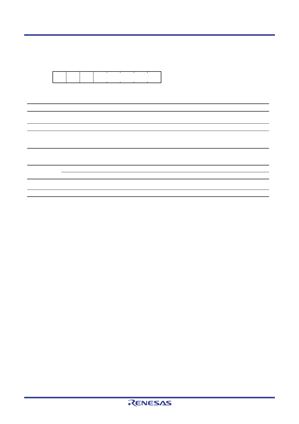
Address(es): PD3PFS 0008 C1ABh
b7 b6 b5 b4 b3 b2 b1 b0
ASEL ISEL — PSEL[4:0]
Value after reset:
00000000
Bit Symbol Bit Name Description R/W
b4 to b0 PSEL[4:0] Pin Function Select These bits select the peripheral function. For individual pin functions,
see the tables below.
R/W
b6, b5 — Reserved These bits are read as 0. The write value should be 0. R/W
b7 ASEL Analog Function Select 0: Used other than as analog pin
1: Used as analog pin
PD3: AN027 (85/56 pins)
R/W
Table 22.10 Register Settings for Input/Output Pin Function in 85-Pin and 56-Pin
PSEL[4:0]
Settings
Pin
PD3
00000b
(initial value)
Hi-Z
00111b POE8#

 Loading...


