R01UH0823EJ0100 Rev.1.00 Page 1774 of 1823
Jul 31, 2019
RX23W Group 51. Electrical Characteristics
51.3.3 Timing of Recovery from Low Power Consumption Modes
Note 1. The recovery time varies depending on the state of each oscillator when the WAIT instruction is executed. When multiple
oscillators are operating, the recovery time varies depending on the operating state of the oscillators that are not selected as the
system clock source. The above table applies when only the corresponding clock is operating.
Note 2. When the frequency of the crystal is 20 MHz.
When the main clock oscillator wait control register (MOSCWTCR) is set to 04h.
Note 3. When the frequency of the external clock is 20 MHz.
When the main clock oscillator wait control register (MOSCWTCR) is set to 00h.
Note 1. The recovery time varies depending on the state of each oscillator when the WAIT instruction is executed. When multiple
oscillators are operating, the recovery time varies depending on the operating state of the oscillators that are not selected as the
system clock source. The above table applies when only the corresponding clock is operating.
Note 2. When the frequency of the crystal is 12 MHz.
When the main clock oscillator wait control register (MOSCWTCR) is set to 04h.
Note 3. When the frequency of PLL is 12 MHz.
When the main clock oscillator wait control register (MOSCWTCR) is set to 04h.
Note 4. When the frequency of the external clock is 12 MHz.
When the main clock oscillator wait control register (MOSCWTCR) is set to 00h.
Note 5. When the frequency of PLL is 12 MHz.
When the main clock oscillator wait control register (MOSCWTCR) is set to 00h.
Note 6. This is the case when HOCO is selected as the system clock and its frequency division is set to be 8 MHz.
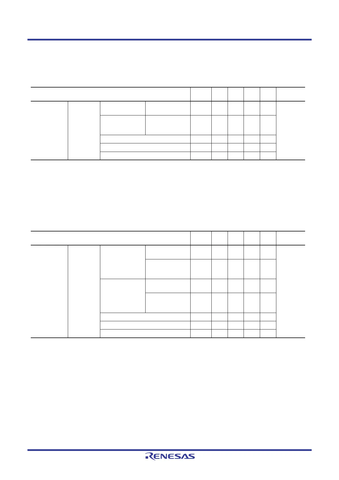
Table 51.26 Timing of Recovery from Low Power Consumption Modes (1)
Conditions: 1.8 V ≤ VCC = VCC_USB = AVCC0 = VCC_RF = AVCC_RF ≤ 3.6 V, VSS = AVSS0 = VSS_USB = VSS_RF = 0 V,
T
a
= –40 to +85°C
Item Symbol Min. Typ. Max. Unit
Test
Conditions
Recovery time
from software
standby mode*
1
High-speed
mode
Crystal connected to
main clock oscillator
Main clock oscillator
operating*
2
t
SBYMC
— 2 3 ms Figure 51.30
External clock input
to main clock
oscillator
Main clock oscillator
operating*
3
t
SBYEX
—3550μs
Sub-clock oscillator operating t
SBYSC
— 650 800 μs
HOCO clock oscillator operating t
SBYHO
—4055μs
LOCO clock oscillator operating t
SBYLO
—4055μs
Table 51.27 Timing of Recovery from Low Power Consumption Modes (2)
Conditions: 1.8 V ≤ VCC = VCC_USB = AVCC0 = VCC_RF = AVCC_RF ≤ 3.6 V, VSS = AVSS0 = VSS_USB = VSS_RF = 0 V,
T
a
= –40 to +85°C
Item Symbol Min. Typ. Max. Unit
Test
Conditions
Recovery time
from software
standby mode*
1
Middle-speed
mode
Crystal connected to
main clock oscillator
Main clock oscillator
operating*
2
t
SBYMC
— 2 3 ms Figure 51.30
Main clock oscillator
and PLL circuit
operating*
3
t
SBYPC
—2 3ms
External clock input
to main clock
oscillator
Main clock oscillator
operating*
4
t
SBYEX
—3 4μs
Main clock oscillator
and PLL circuit
operating*
5
t
SBYPE
—6585μs
Sub-clock oscillator operating t
SBYSC
— 600 750 μs
HOCO clock oscillator operating*
6
t
SBYHO
—4050μs
LOCO clock oscillator operating t
SBYLO
—5 7μs

 Loading...


