R01UH0823EJ0100 Rev.1.00 Page 172 of 1823
Jul 31, 2019
RX23W Group 9. Clock Generation Circuit
9.2 Register Descriptions
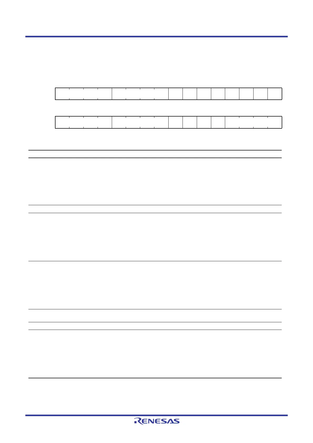
9.2.1 System Clock Control Register (SCKCR)
Address(es): 0008 0020h
b31 b30 b29 b28 b27 b26 b25 b24 b23 b22 b21 b20 b19 b18 b17 b16
FCK[3:0] ICK[3:0] ————————
Value after reset:
0011001100000011
b15 b14 b13 b12 b11 b10 b9 b8 b7 b6 b5 b4 b3 b2 b1 b0
PCKA[3:0] PCKB[3:0] ———— PCKD[3:0]
Value after reset:
0011001100000011
Bit Symbol Bit Name Description R/W
b3 to b0 PCKD[3:0]
Peripheral Module Clock D
(PCLKD) Select
b3 b0
0 0 0 0: ×1
0 0 0 1: ×1/2
0 0 1 0: ×1/4
0 0 1 1: ×1/8
0 1 0 0: ×1/16
0 1 0 1: ×1/32
0 1 1 0: ×1/64
Settings other than above are prohibited.
R/W
b7 to b4 —
Reserved
These bits are read as 0. The write value should be 0. R/W
b11 to b8 PCKB[3:0] Peripheral Module Clock B
(PCLKB) Select
b11 b8
0 0 0 0: ×1
0 0 0 1: ×1/2
0 0 1 0: ×1/4
0 0 1 1: ×1/8
0 1 0 0: ×1/16
0 1 0 1: ×1/32
0 1 1 0: ×1/64
Settings other than above are prohibited.
R/W
b15 to b12 PCKA[3:0] Peripheral Module Clock A
(PCLKA) Select
b15 b12
0 0 0 0: ×1
0 0 0 1: ×1/2
0 0 1 0: ×1/4
0 0 1 1: ×1/8
0 1 0 0: ×1/16
0 1 0 1: ×1/32
0 1 1 0: ×1/64
Settings other than above are prohibited.
R/W
b19 to b16 — Reserved Set the value to whichever is greater of the values of the ICK[3:0] and
PCKB[3:0] bits.
R/W
b23 to b20 — Reserved
These bits are read as 0. The write value should be 0.
R/W
b27 to b24 ICK[3:0]
*
1
System Clock (ICLK)
Select
b27 b24
0 0 0 0: ×1
0 0 0 1: ×1/2
0 0 1 0: ×1/4
0 0 1 1: ×1/8
0 1 0 0: ×1/16
0 1 0 1: ×1/32
0 1 1 0: ×1/64
Settings other than above are prohibited.
R/W

 Loading...


