R01UH0823EJ0100 Rev.1.00 Page 445 of 1823
Jul 31, 2019
RX23W Group 21. I/O Ports
21.3.5 Open Drain Control Register 0 (ODR0)
m = 2, 3, B, C, E, J
Bits corresponding to port m on the 85 pin-product but which do not exist on a product with fewer than 85 pins are
reserved. Write 0 to these bits.
The bits corresponding to a pin that does not exist or pins with no open-drain output allocation are reserved. A reserved
bit is read as 0. The write value should be 0.
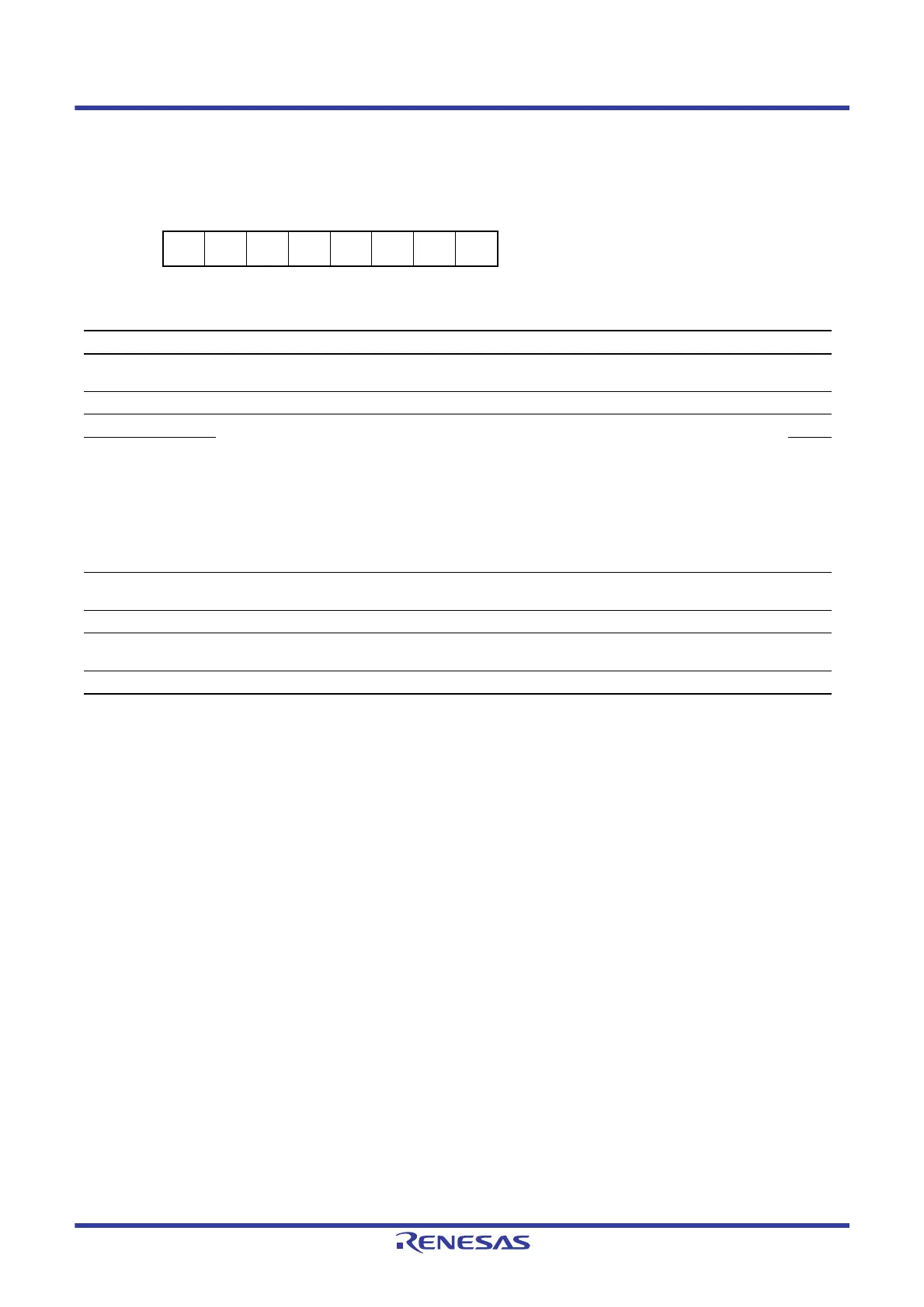
Address(es): PORT2.ODR0 0008 C084h, PORT3.ODR0 0008 C086h, PORTB.ODR0 0008 C096h, PORTC.ODR0 0008 C098h,
PORTE.ODR0 0008 C09Ch, PORTJ.ODR0 0008 C0A4h
b7 b6 b5 b4 b3 b2 b1 b0
B7 B6 B5 B4 B3 B2 B1 B0
Value after reset:
00000000
Bit Symbol Bit Name Description R/W
b0 B0 Pm0 Output Type Select 0: CMOS output
1: N-channel open-drain
R/W
b1 B1 Reserved This bit is read as 0. The write value should be 0. R/W
b2 B2 Pm1 Output Type Select
P21, P31, PB1
b2 0: CMOS output
1: N-channel open-drain
b3 This bit is read as 0. The write value should be 0.
PE1
b3 b2
0 0: CMOS output
0 1: N-channel open-drain
1 0: P-channel open-drain
1 1: Hi-Z
R/W
b3 B3 R/W
b4 B4 Pm2 Output Type Select 0: CMOS output
1: N-channel open-drain
R/W
b5 B5 Reserved This bit is read as 0. The write value should be 0. R/W
b6 B6 Pm3 Output Type Select 0: CMOS output
1: N-channel open-drain
R/W
b7 B7 Reserved This bit is read as 0. The write value should be 0. R/W

 Loading...


