R01UH0823EJ0100 Rev.1.00 Page 718 of 1823
Jul 31, 2019
RX23W Group 25. 16-Bit Timer Pulse Unit (TPUa)
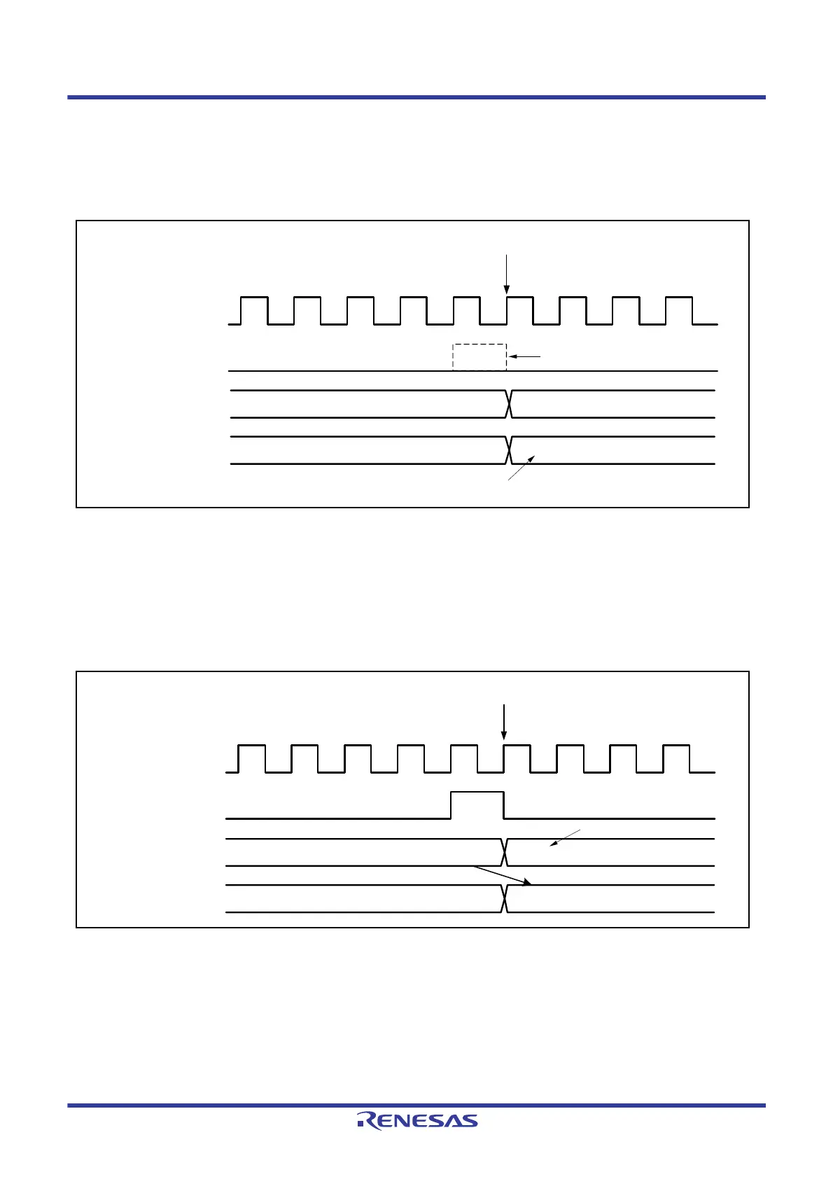
25.9.6 Conflict between TPUm.TGRy Write and Compare Match
If a compare match occurs in a TGRy write cycle, the TGRy write takes precedence and the compare match signal is
disabled. A compare match also does not occur when the same value as before is written.
Figure 25.46 shows the timing in this case.
Figure 25.46 Conflict between TPUm.TGRy Write and Compare Match
25.9.7 Conflict between Buffer Register Write and Compare Match
If a compare match occurs in a TPUm.TGRy write cycle, the data transferred to TGRy by the buffer operation will be the
data before writing.
Figure 25.47 shows the timing in this case.
Figure 25.47 Conflict between Buffer Register Write and Compare Match
TCNT
TGRy
PCLK
Compare match signal
M
N
TGR write by CPU
Disabled
N + 1
TGRy write data
N
Buffer register
TGRy
PCLK
Compare match signal
Buffer register write by CPU
MN
Buffer register write data
N

 Loading...


