R01UH0823EJ0100 Rev.1.00 Page 177 of 1823
Jul 31, 2019
RX23W Group 9. Clock Generation Circuit
9.2.5 USB-dedicated PLL Control Register (UPLLCR)
Note: Set the PRCR.PRC0 bit to 1 (write enabled) before rewriting this register.
Writing to the UPLLCR is prohibited when the UPLLCR2.UPLLEN bit is 0 (USB-dedicated PLL is operating).
UPLIDIV[1:0] Bits (USB-dedicated PLL Input Frequency Division Ratio Select)
These bits select the input frequency division ratio of the USB-dedicated PLL clock source.
Set these bits so that the input frequency of the USB-dedicated PLL input is 4, 6, 8, 12 MHz.
UCKUPLLSEL Bit (UCLK Source USB-Dedicated PLL Select)
This bit selects the USB-dedicated PLL clock. When this bit is set to 1, the USB-dedicated PLL (48 MHz) is supplied to
the UCLK, and the clock of the oscillator (up to 54 MHz) selected by the SCKCR3.CKSEL[2:0] bits is supplied to the
system clock.
When setting this bit to change the UCLK source clock, set the MSTPCRB.MSTPB19 bit (this module clock is disabled)
and wait for at least three cycles of the clock before the change.
USTC[5:0] Bits (Frequency Multiplication Factor Select)
These bits select the frequency multiplication factor of the USB-dedicated PLL circuit.
Set these bits so that the USB-dedicated PLL oscillation frequency is 48 MHz.
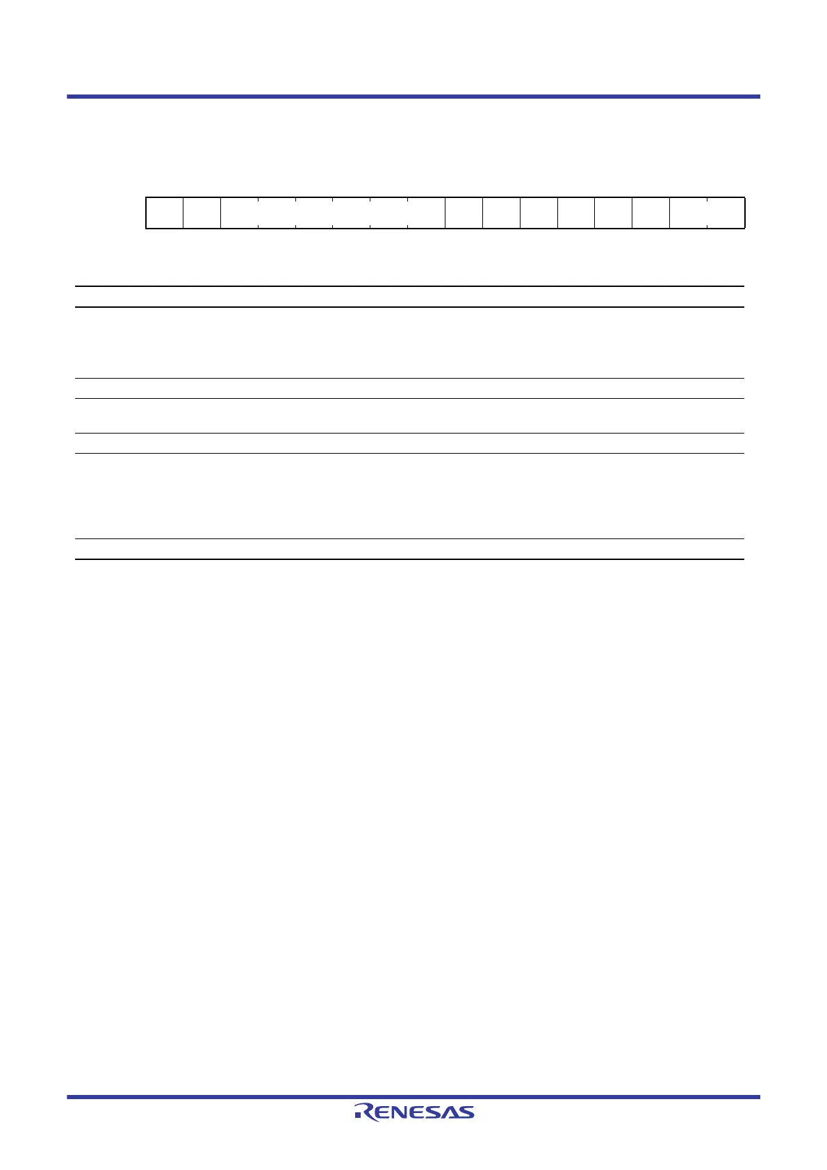
Address(es): 0008 002Ch
b15 b14 b13 b12 b11 b10 b9 b8 b7 b6 b5 b4 b3 b2 b1 b0
—— USTC[5:0] ———
UCKUP
LLSEL
— — UPLIDIV[1:0]
Value after reset:
0000111100000000
Bit Symbol Bit Name Description R/W
b1, b0 UPLIDIV[1:0] USB-dedicated PLL Input
Frequency Division Ratio Select
b1 b0
0 0: ×1
0 1: ×1/2
1 0: ×1/4
Settings other than above are prohibited.
R/W
b3, b2 — Reserved These bits are read as 0. The write value should be 0. R/W
b4 UCKUPLLSEL UCLK Source USB-Dedicated
PLL Select
0: System clock is selected as UCLK
1: USB-dedicated PLL is selected as UCLK
R/W
b7 to b5 — Reserved These bits are read as 0. The write value should be 0. R/W
b13 to b8 USTC[5:0] Frequency Multiplication Factor
Select
b13 b8
0 0 0 1 1 1: ×4
0 0 1 0 1 1: ×6
0 0 1 1 1 1: ×8
0 1 0 1 1 1: ×12
Settings other than above are prohibited.
R/W
b15, b14 — Reserved These bits are read as 0. The write value should be 0. R/W

 Loading...


