R01UH0823EJ0100 Rev.1.00 Page 1535 of 1823
Jul 31, 2019
RX23W Group 44. 12-Bit A/D Converter (S12ADE)
44.2 Register Descriptions
44.2.1 A/D Data Registers y (ADDRy) (y = 0 to 7, 16 to 20, 27),
A/D Data Duplication Register (ADDBLDR),
A/D Temperature Sensor Data Register (ADTSDR),
A/D Internal Reference Voltage Data Register (ADOCDR)
ADDRy (y = 0 to 7, 16 to 20, 27) are 16-bit read-only registers which store the A/D conversion results.
ADDBLDR is a 16-bit read-only register used in double trigger mode. ADDBLDR stores the results of A/D conversion
when the conversion is started by the second trigger.
ADTSDR is a 16-bit read-only register that stores the A/D conversion results of the temperature sensor output.
ADOCDR is a 16-bit read-only register that stores the A/D conversion results of the internal reference voltage.
The format of each register differs depending on the conditions below.
Settings of the A/D data register format select bit (ADCER.ADRFMT) (flush-right or flush-left)
Settings of the addition count select bits (ADADC.ADC[2:0]) (addition once, twice, three, or 15 times)
Settings of the average mode enable bit (ADADC.AVEE) (addition or average)
The data formats for each given condition are shown below.
(1) When A/D-Converted Value Addition/Average Mode is Not Selected
Flush-right format
The A/D-converted value is stored in bits 11 to 0. Bits 15 to 12 are read as 0.
Flush-left format
The A/D-converted value is stored in bits 15 to 4. Bits 3 to 0 are read as 0.
(2) When A/D-Converted Average Mode is Selected
Flush-right format
The mean value of the A/D-converted results of the same channel is stored in bits 11 to 0.
Bits 15 to 12 are read as 0.
Flush-left format
The mean value of the A/D-converted results of the same channel is stored in bits 15 to 4.
Bits 3 to 0 are read as 0.
A/D-converted value average mode can be set only when twice or four times is selected in A/D-converted value addition
mode.
(3) When A/D-Converted Value Addition Mode is Selected
Flush-right format (A/D-converted value addition mode and 1-time to 4-time conversion selected)
The value added by the A/D-converted value of the same channel is stored in bits 13 to 0.
Bits 15 and 14 are read as 0.
Flush-right format (A/D-converted value addition mode and 16-time conversion selected)
The value added by the A/D-converted value of the same channel is stored in bits 15 to 0.
Flush-left format (A/D-converted value addition mode and 1-time to 4-time conversion selected)
Address(es): S12AD.ADDR0 0008 9020h, S12AD.ADDR1 0008 9022h, S12AD.ADDR2 0008 9024h,
S12AD.ADDR3 0008 9026h, S12AD.ADDR4 0008 9028h, S12AD.ADDR5 0008 902Ah,
S12AD.ADDR6 0008 902Ch, S12AD.ADDR7 0008 902Eh, S12AD.ADDR16 0008 9040h,
S12AD.ADDR17 0008 9042h, S12AD.ADDR18 0008 9044h, S12AD.ADDR19 0008 9046h,
S12AD.ADDR20 0008 9048h, S12AD.ADDR27 0008 9056h,S12AD.ADDBLDR 0008 9018h,
S12AD.ADTSDR 0008 901Ah, S12AD.ADOCDR 0008 901Ch
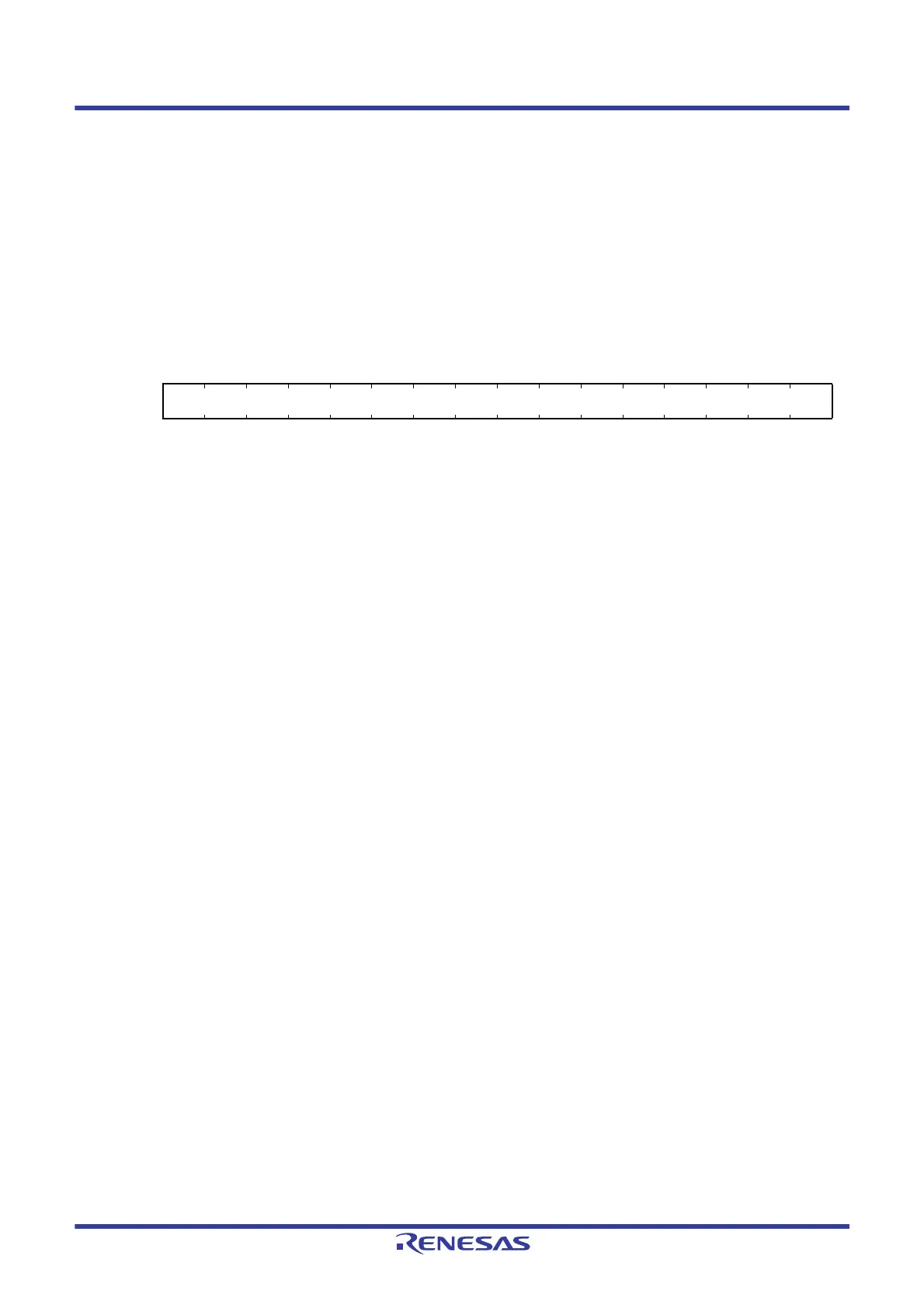
b15 b14 b13 b12 b11 b10 b9 b8 b7 b6 b5 b4 b3 b2 b1 b0
Value after reset:
0000000000000000

 Loading...