R01UH0823EJ0100 Rev.1.00 Page 1792 of 1823
Jul 31, 2019
RX23W Group 51. Electrical Characteristics
51.4 USB Characteristics
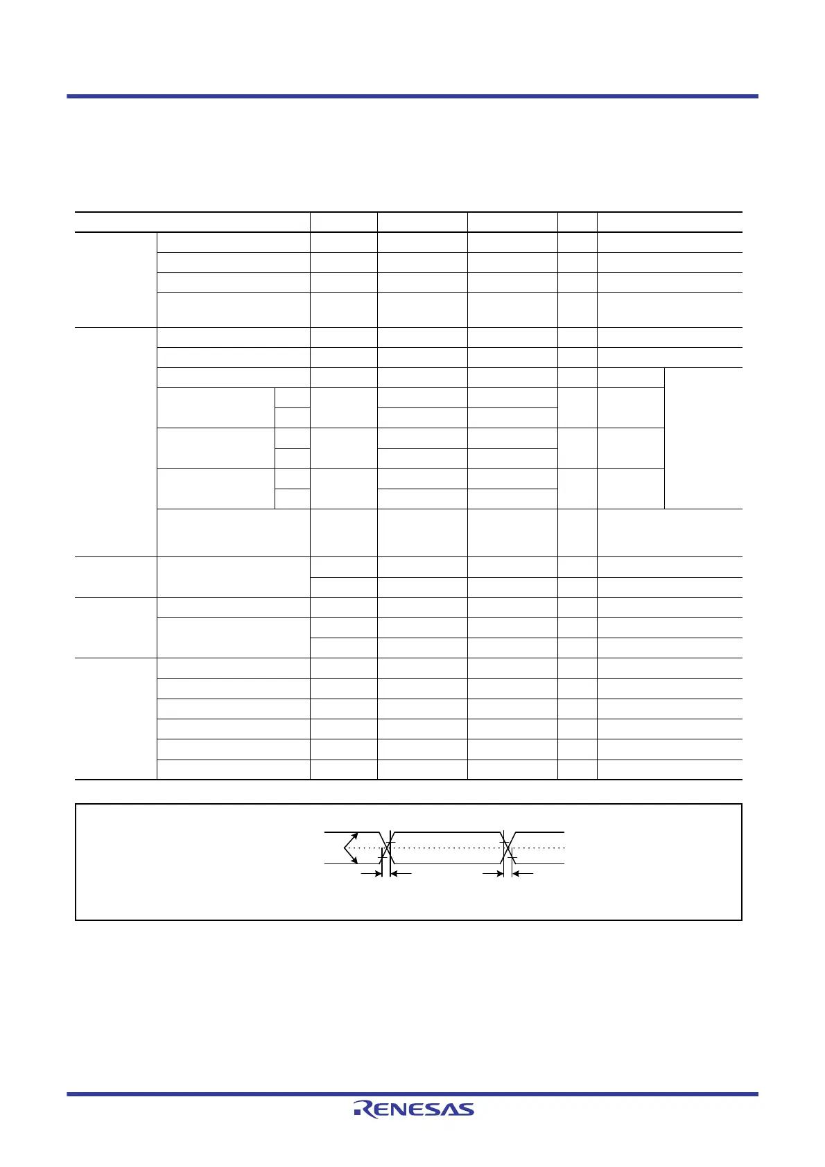
Figure 51.55 USB0_DP and USB0_DM Output Timing
Table 51.39 USB Characteristics (USB0_DP and USB0_DM Pin Characteristics)
Conditions: 3.0 V ≤ VCC = VCC_USB = AVCC = VCC_RF = AVCC_RF < 3.6 V, VSS = AVSS0 = VSS_USB = VSS_RF = 0 V,
T
a
= –40 to +85°C
Item Symbol Min. Max. Unit Test Conditions
Input
characteristics
Input high level voltage V
IH
2.0 — V
Input low level voltage V
IL
—0.8V
Differential input sensitivity V
DI
0.2 — V | USB0_DP – USB0_DM |
Differential common mode
range
V
CM
0.8 2.5 V
Output
characteristics
Output high level voltage V
OH
2.8 VCC_USB V I
OH
= –200 μA
Output low level voltage V
OL
0.0 0.3 V I
OL
= 2 mA
Cross-over voltage V
CRS
1.3 2.0 V Figure 51.55,
Figure 51.56
Rise time FS t
r
420ns
LS 75 300
Fall time FS t
f
420ns
LS 75 300
Rise/fall time ratio FS t
r
/t
f
90 111.11 % t
r
/t
f
LS 80 125
Output resistance Z
DRV
28 44 Ω (Adjusting the resistance by
external elements is not
necessary.)
VBUS
characteristics
VBUS input voltage V
IH
VCC × 0.8 — V
V
IL
— VCC × 0.2 V
Pull-up,
pull-down
Pull-down resistor R
PD
14.25 24.80 kΩ
Pull-up resistor R
PUI
0.9 1.575 kΩ During idle state
R
PUA
1.425 3.09 kΩ During reception
Battery
Charging
Specification
Ver 1.2
D+ sink current I
DP_SINK
25 175 μA
D- sink current I
DM_SINK
25 175 μA
DCD source current I
DP_SRC
713μA
Data detection voltage V
DAT_REF
0.25 0.4 V
D+ source current V
DP_SRC
0.5 0.7 V Output current = 250 μA
D- source current V
DM_SRC
0.5 0.7 V Output current = 250 μA
USB0_DP,
USB0_DM
t
f
t
r
90%
10%10%
90%
V
CRS

 Loading...


