R01UH0823EJ0100 Rev.1.00 Page 1808 of 1823
Jul 31, 2019
RX23W Group 51. Electrical Characteristics
Figure 51.66 Voltage Detection Circuit Timing (V
det1
)
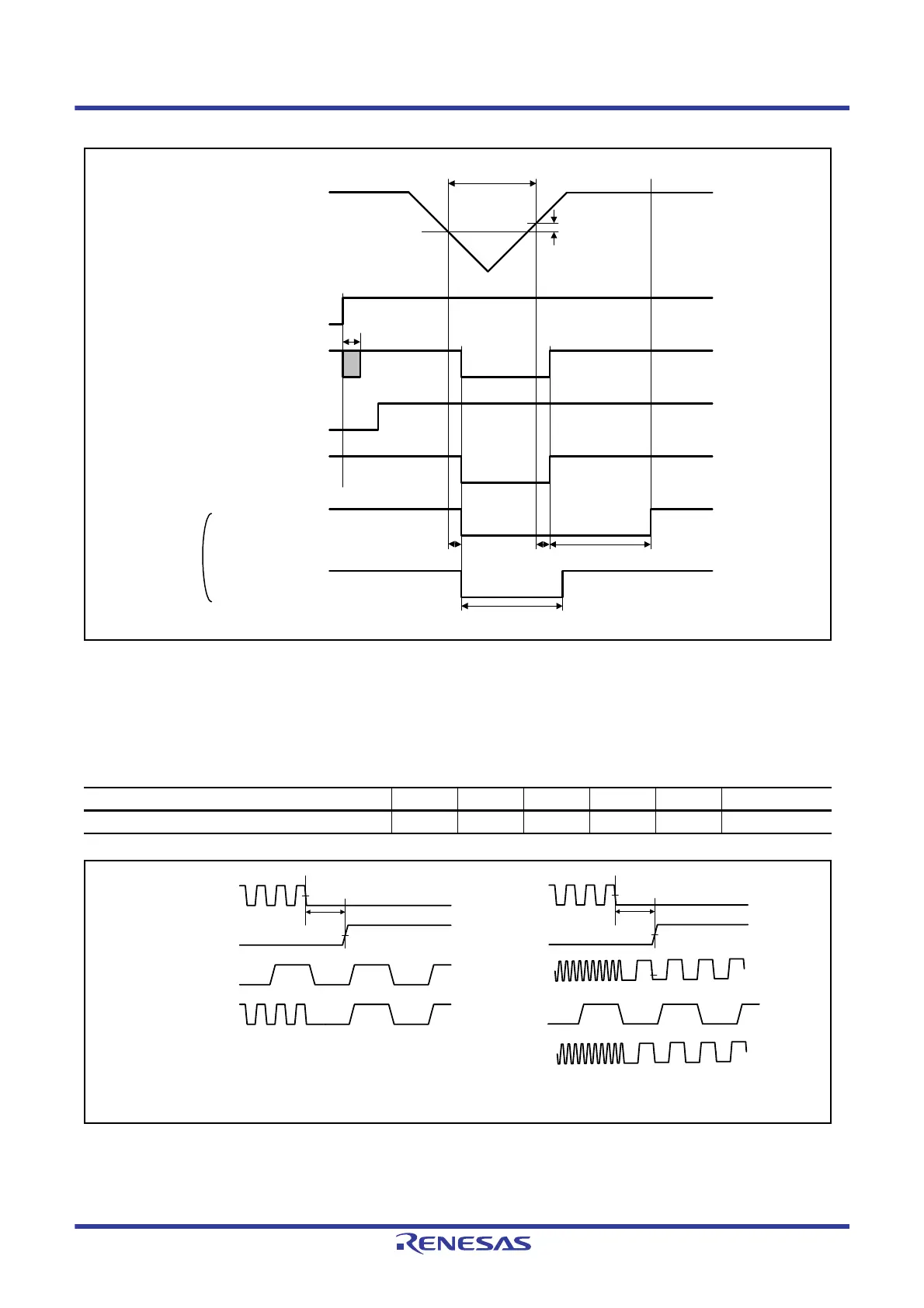
51.11 Oscillation Stop Detection Timing
Figure 51.67 Oscillation Stop Detection Timing
Table 51.53 Oscillation Stop Detection Timing
Conditions: 1.8 V ≤ VCC = VCC_USB = AVCC0 = VCC_RF = AVCC_RF ≤ 3.6 V,
VSS = AVSS0 = VREFL0 = VSS_USB = VSS_RF = 0 V, T
a
= –40 to +85°C
Item Symbol Min. Typ. Max. Unit Test Conditions
Detection time t
dr
— — 1 ms Figure 51.67
t
VOFF
V
det1
VCC
t
det
t
det
t
LVD1
T
d(E-A)
LVD1E
LVD1
Comparator output
LVD1CMPE
LVD1MON
Internal reset signal
(active-low)
When LVD1RN = L
When LVD1RN = H
V
LVH
t
LVD1
t
dr
Main clock
OSTDSR.OSTDF
Low-speed clock
ICLK
t
dr
Main clock
OSTDSR.OSTDF
ICLK
When the main clock is selected
When the PLL clock is selected
PLL clock
Low-speed clock

 Loading...


