R01UH0823EJ0100 Rev.1.00 Page 1666 of 1823
Jul 31, 2019
RX23W Group 50. Flash Memory (FLASH)
Wait for ROM mode transition wait time 2 (tMS, refer to section 51, Electrical Characteristics).
RPDIS Bit (ROM P/E Disable)
This bit is used to disable the execution of ROM programming/erasure with software.
LVPE Bit (Low-Voltage P/E Mode Enable)
Set this bit to 0 for programming/erasure in high-speed mode, and set this bit to 1 for programming/erasure in middle-
speed mode.
50.4.6 Flash Initial Setting Register (FISR)
x: Don’t care
Data can be written to the FISR register in ROM P/E mode or E2 DataFlash P/E mode.
PCKA[4:0] Bits (Peripheral Clock Notification)
These bits are used to set the frequency of the FlashIF clock (FCLK) when programming/erasing the ROM/E2
DataFlash.
Set the FCLK frequency in the PCKA[4:0] bits before programming/erasure. Do not change the frequency during
programming/erasure of the ROM/E2 DataFlash.
[When FCLK is higher than 4 MHz]
Set a rounded-up value for a non-integer frequency.
For example, set 32 MHz (PCKA[4:0] bits = 11111b) when the frequency is 31.5 MHz.
[When FCLK is 4 MH or lower]
Do not use a non-integer frequency.
Use the FCLK at a frequency of 1, 2, 3, or 4 MHz.
Note: When the PCKA[4:0] bits are set to a frequency different from the FCLK, the data in the ROM/E2 DataFlash may
be damaged.
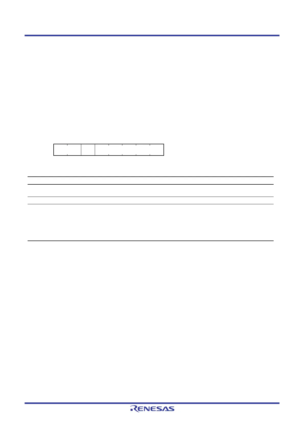
Address(es): FLASH.FISR 007F C1D8h
b7 b6 b5 b4 b3 b2 b1 b0
SAS[1:0] — PCKA[4:0]
Value after reset:
00000000
Bit Symbol Bit Name Description R/W
b4 to b0 PCKA[4:0] Peripheral Clock Notification These bits are used to set the frequency of the FlashIF clock
(FCLK).
R/W
b5 — Reserved This bit is read as 0. The write value should be 0. R/W
b7, b6 SAS[1:0] Start-Up Area Select
b7 b6
0 x: The start-up area is selected according to the start-up
area settings of the extra area.
1 0: The start-up area is switched to the default area
temporarily.
1 1: The start-up area is switched to the alternate area
temporarily.
R/W

 Loading...


