R01UH0823EJ0100 Rev.1.00 Page 1499 of 1823
Jul 31, 2019
RX23W Group 43. Capacitive Touch Sensing Unit (CTSU)
43.2.7 CTSU Channel Enable Control Register n (CTSUCHACn) (n = 0 to 3)
Note 1. TS0, TS1, TS5, TS6, TS9, TS10, TS11, TS14, TS15, TS16, TS17, TS18, TS19, TS20, TS21, TS24, TS25, TS26, TS28, TS29,
and TS31 pins are not available.
The CTSUCHACn register should be set when the CTSUCR0.CTSUSTRT bit is 0.
CTSUCHACnj Bit (CTSU Channel Enable Control nj) (j = 0 to 7)
This bit sets the pin (for receive and transmit) whose electrostatic capacitance is to be measured.
CTSUCHAC00 bit corresponds to TS0 pin and CTSUCHAC07 bit corresponds to TS7 pin.
CTSUCHAC10 bit corresponds to TS8 pin and CTSUCHAC17 bit corresponds to TS15 pin.
CTSUCHAC20 bit corresponds to TS16 pin and CTSUCHAC27 bit corresponds to TS23 pin.
CTSUCHAC30 bit corresponds to TS24 pin and CTSUCHAC37 bit corresponds to TS31 pin.
Note: TS0, TS1, TS5, TS6, TS9, TS10, TS11, TS14, TS15, TS16, TS17, TS18, TS19, TS20, TS21, TS24, TS25, TS26,
TS28, TS29, and TS31 pins are not available.
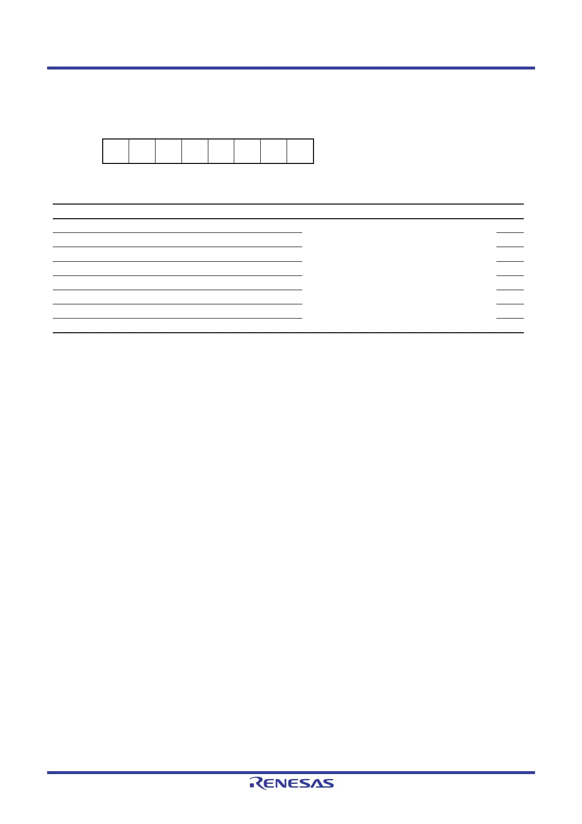
Address(es): CTSU.CTSUCHAC0 000A 0906h, CTSU.CTSUCHAC1 000A 0907h, CTSU.CTSUCHAC2 000A 0908h, CTSU.CTSUCHAC3 000A 0909h
b7 b6 b5 b4 b3 b2 b1 b0
CTSUC
HACn7
CTSUC
HACn6
CTSUC
HACn5
CTSUC
HACn4
CTSUC
HACn3
CTSUC
HACn2
CTSUC
HACn1
CTSUC
HACn0
Value after reset:
00000000
Bit Symbol Bit Name Description R/W
b0 CTSUCHACn0 CTSU Channel Enable Control n0 0: Not measurement target
1: Measurement target
These bits specify the TS0 to TS31 pins*
1
.
R/W
b1 CTSUCHACn1 CTSU Channel Enable Control n1 R/W
b2 CTSUCHACn2 CTSU Channel Enable Control n2 R/W
b3 CTSUCHACn3 CTSU Channel Enable Control n3 R/W
b4 CTSUCHACn4 CTSU Channel Enable Control n4 R/W
b5 CTSUCHACn5 CTSU Channel Enable Control n5 R/W
b6 CTSUCHACn6 CTSU Channel Enable Control n6 R/W
b7 CTSUCHACn7 CTSU Channel Enable Control n7 R/W

 Loading...


