R01UH0823EJ0100 Rev.1.00 Page 502 of 1823
Jul 31, 2019
RX23W Group 23. Multi-Function Timer Pulse Unit 2 (MTU2a)
23.2.15 Timer Read/Write Enable Registers (TRWER)
The TRWER registers enable or disable access to the registers and counters that have write-protection capability against
accidental modification in MTU3 and MTU4.
RWE Bit (Read/Write Enable)
This bit enables or disables access to the registers that have write-protection capability against accidental modification.
[Clearing condition]
When 0 is written to the RWE bit after reading the RWE bit = 1
Registers and Counters having Write-Protection Capability against Accidental Modification
22 registers: MTUn.TCR, MTUn.TMDR, MTUn.TIORH, MTUn.TIORL, MTUn.TIER, MTUn.TGRA, MTUn.TGRB,
MTU.TOER, MTU.TOCR1, MTU.TOCR2, MTU.TGCR, MTU.TCDR, MTU.TDDR, and MTUn.TCNT (n = 3, 4)
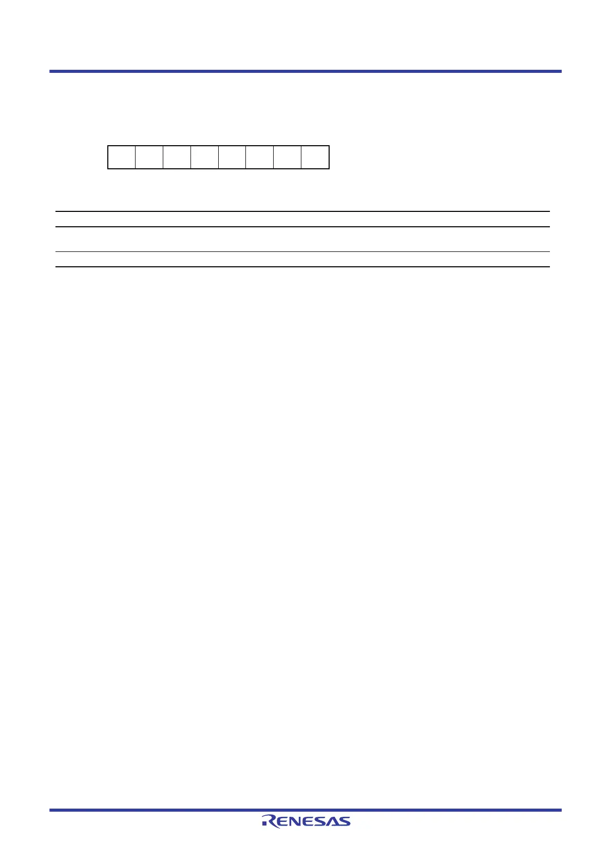
Address(es): MTU.TRWER 000D 0A84h
b7 b6 b5 b4 b3 b2 b1 b0
———————RWE
Value after reset:
00000001
Bit Symbol Bit Name Description R/W
b0 RWE Read/Write Enable 0: Read/write access to the registers is disabled
1: Read/write access to the registers is enabled
R/W
b7 to b1 — Reserved These bits are read as 0. The write value should be 0. R/W

 Loading...


