R01UH0823EJ0100 Rev.1.00 Page 494 of 1823
Jul 31, 2019
RX23W Group 23. Multi-Function Timer Pulse Unit 2 (MTU2a)
23.2.6 Timer Buffer Operation Transfer Mode Register (TBTM)
MTU0.TBTM
MTU3.TBTM, MTU4.TBTM
The MTU has a total of three TBTM registers, one each for MTU0, MTU3, and MTU4.
The TBTM register specifies the timing for transferring data from the buffer register to the timer general register in
PWM mode.
TTSA Bit (Timing Select A)
This bit specifies the timing for transferring data from the TGRC register to the TGRA register in each channel when
they are used together for buffer operation. When a channel is not set to PWM mode, do not set the TTSA bit in the
channel to 1.
TTSB Bit (Timing Select B)
This bit specifies the timing for transferring data from the TGRD register to the TGRB register in each channel when
they are used together for buffer operation. When a channel is not set to PWM mode, do not set the TTSB bit in the
channel to 1.
TTSE Bit (Timing Select E)
This bit specifies the timing for transferring data from the MTU0.TGRF register to the MTU0.TGRE register when they
are used together for buffer operation. In MTU3 and MTU4, this bit is reserved and read as 0. The write value should be
0. When MTU0 is not set to PWM mode, do not set the TTSE bit to 1.
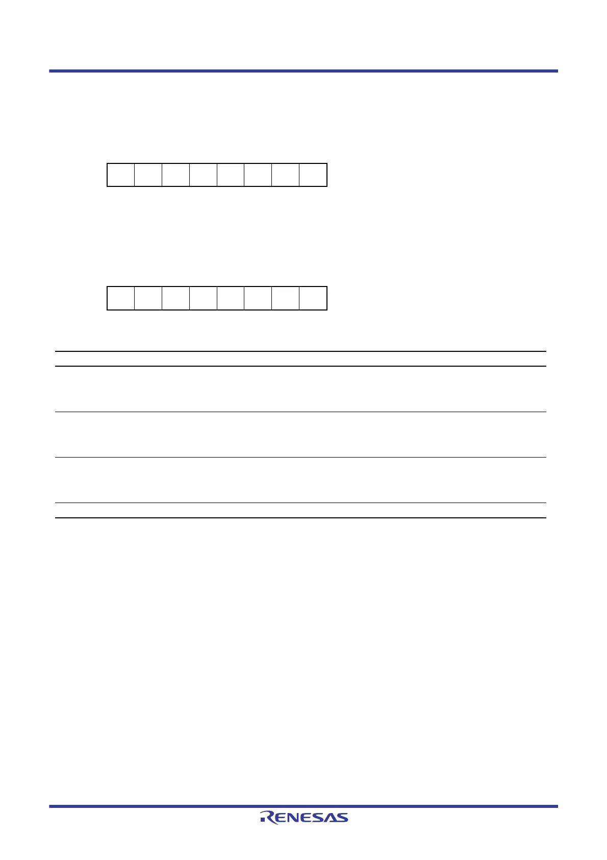
Address(es): MTU0.TBTM 000D 0B26h
b7 b6 b5 b4 b3 b2 b1 b0
—————TTSETTSBTTSA
Value after reset:
00000000
Address(es): MTU3.TBTM 000D 0A38h, MTU4.TBTM 000D 0A39h
b7 b6 b5 b4 b3 b2 b1 b0
——————TTSBTTSA
Value after reset:
00000000
Bit Symbol Bit Name Description R/W
b0 TTSA Timing Select A 0: When compare match A occurs in each channel, data is transferred
from TGRC to TGRA
1: When TCNT is cleared in each channel, data is transferred from TGRC
to TGRA
R/W
b1 TTSB Timing Select B 0: When compare match B occurs in each channel, data is transferred
from TGRD to TGRB
1: When TCNT is cleared in each channel, data is transferred from TGRD
to TGRB
R/W
b2 TTSE Timing Select E 0: When compare match E occurs in MTU0, data is transferred from
MTU0.TGRF to MTU0.TGRE
1: When MTU0.TCNT is cleared in MTU0, data is transferred from
MTU0.TGRF to MTU0.TGRE
R/W
b7 to b3 — Reserved These bits are read as 0. The write value should be 0. R/W

 Loading...


