R01UH0823EJ0100 Rev.1.00 Page 459 of 1823
Jul 31, 2019
RX23W Group 22. Multi-Function Pin Controller (MPC)
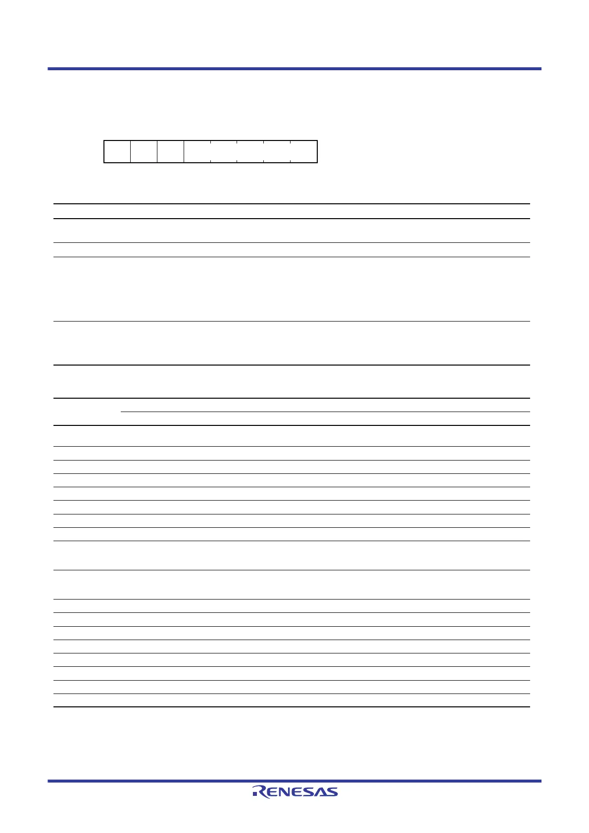
22.2.3 P1n Pin Function Control Registers (P1nPFS) (n = 4 to 7)
—: Do not specify this value.
Address(es): P14PFS 0008 C14Ch, P15PFS 0008 C14Dh, P16PFS 0008 C14Eh, P17PFS 0008 C14Fh
b7 b6 b5 b4 b3 b2 b1 b0
ASEL ISEL — PSEL[4:0]
Value after reset:
00000000
Bit Symbol Bit Name Description R/W
b4 to b0 PSEL[4:0] Pin Function Select These bits select the peripheral function. For individual pin functions,
see the tables below.
R/W
b5 — Reserved This bit is read as 0. The write value should be 0. R/W
b6 ISEL Interrupt Function Select 0: Not used as IRQn input pin
1: Used as IRQn input pin
P14: IRQ4 input switch (85/56 pins)
P15: IRQ5 input switch (85/56 pins)
P16: IRQ6 input switch (85/56 pins)
P17: IRQ7 input switch (85/56 pins)
R/W
b7 ASEL Analog Function Select 0: Used other than as analog pin
1: Used as analog pin
P14: CVREFB2 (85/56 pins)
P15: CMPB2 (85/56 pins)
R/W
Table 22.3 Register Settings for Input/Output Pin Function in 85-Pin and 56-Pin
PSEL[4:0]
Settings
Pin
P14 P15 P16 P17
00000b
(initial value)
Hi-Z
00001b MTIOC3A MTIOC0B MTIOC3C MTIOC3A
00010b MTCLKA MTCLKB MTIOC3D MTIOC3B
00011b TIOCB5 TIOCB2 TIOCB1 TIOCB0
00100b TCLKA TCLKB TCLKC TCLKD
00101b TMRI2 TMCI2 TMO2 TMO1
00111b — — RTCOUT POE8#
01001b — — ADTRG0# —
01010b — RXD1
SMISO1
SSCL1
TXD1
SMOSI1
SSDA1
SCK1
01011b CTS1#
RTS1#
SS1#
———
01101b — — MOSIA MISOA
01111b — — SCL SDA
10000b CTXD0 CRXD0 — CMPOB2
10001b USB0_OVRCURA — USB0_VBUS —
10010b — — USB0_VBUSEN —
10011b — — USB0_OVRCURB —
10111b — — — SSITXD0
11001b TS13 TS12 — —

 Loading...


