R01UH0823EJ0100 Rev.1.00 Page 600 of 1823
Jul 31, 2019
RX23W Group 23. Multi-Function Timer Pulse Unit 2 (MTU2a)
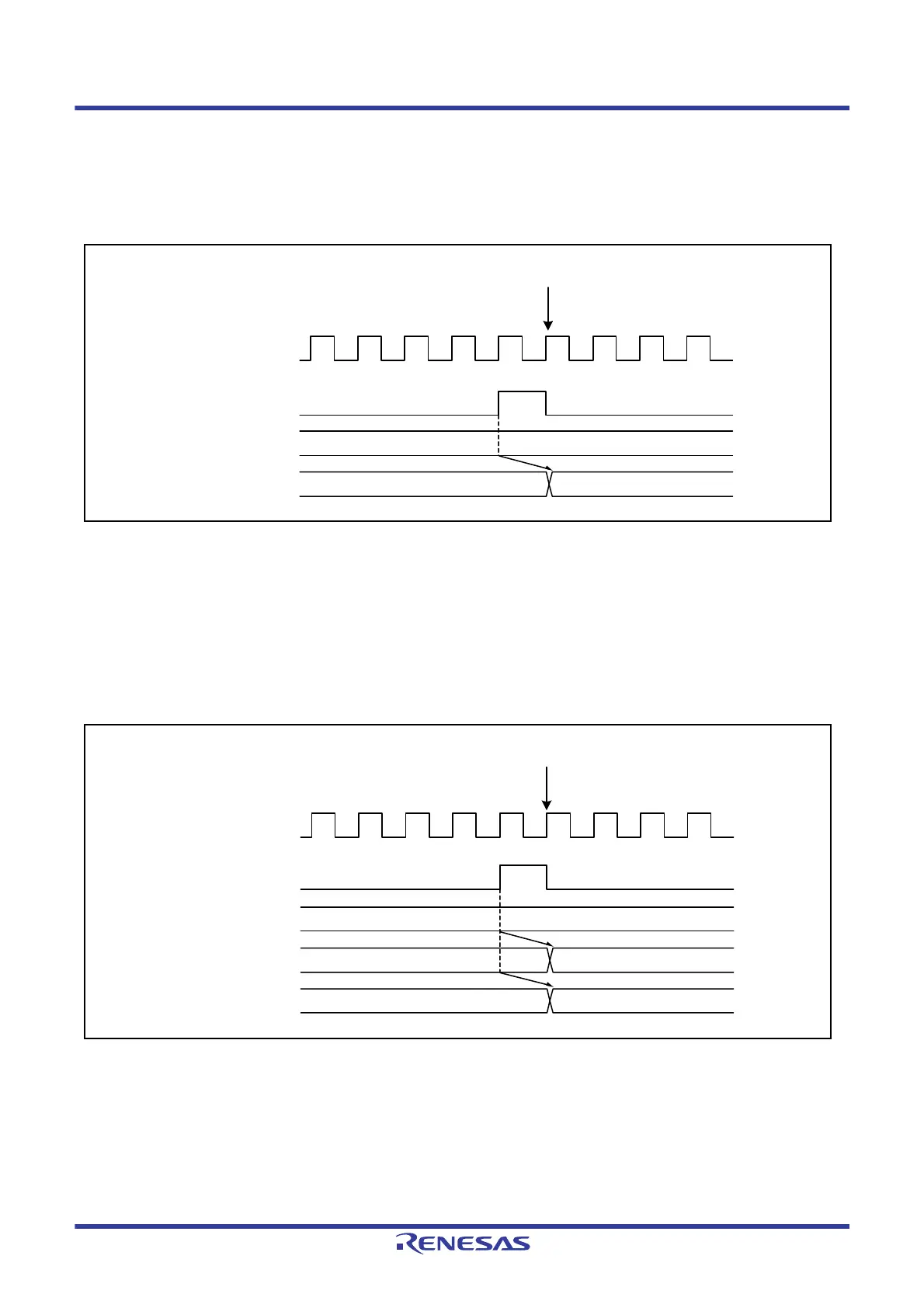
23.6.10 Contention between TGR Write Operation and Input Capture
If an input capture signal is generated in a TGR write cycle, the input capture operation takes precedence and the TGR
register write operation is not performed.
Figure 23.103 show the timing in this case.
Figure 23.103 Contention between TGR Write Operation and Input Capture (MTU0 to MTU4)
23.6.11 Contention between Buffer Register Write Operation and Input Capture
If an input capture signal is generated in a buffer register write cycle, the buffer operation takes precedence and the buffer
register write operation is not performed.
Figure 23.104 shows the timing in this case.
Figure 23.104 Contention between Buffer Register Write Operation and Input Capture
PCLK
Input capture signal
TCNT
TGR
M
M
Written by CPU
Input capture signal
TCNT
TGR
Buffer register
PCLK
N
N
M
M
Written by CPU

 Loading...


