R01UH0823EJ0100 Rev.1.00 Page 1622 of 1823
Jul 31, 2019
RX23W Group 45. 12-Bit D/A Converter (R12DAA)
45.2.2 D/A Control Register (DACR)
This register should be set when the DAADSCR.DAADST bit is 1 (measure against interference between D/A and A/D
conversion is enabled) while the 12-bit A/D converter is halted (the ADCSR.ADST bit is 0). At that time, the software
trigger should be selected for the 12-bit A/D converter trigger to securely stop the 12-bit A/D converter.
45.2.3 Data Register Format Select Register (DADPR)
Address(es): DA.DACR 0008 8044h
b7 b6 b5 b4 b3 b2 b1 b0
DAOE1DAOE0——————
Value after reset:
00011111
Bit Symbol Bit Name Description R/W
b4 to b0 — Reserved These bits are read as 1. The write value should be 1. R/W
b5 — Reserved This bit is read as 0. The write value should be 0. R
b6 DAOE0 D/A Output Enable 0 0: Analog output of channel 0 (DA0) is disabled.
1: D/A conversion of channel 0 is enabled.
Analog output of channel 0 (DA0) is enabled.
R/W
b7 DAOE1 D/A Output Enable 1 0: Analog output of channel 1 (DA1) is disabled.
1: D/A conversion of channel 1 is enabled.
Analog output of channel 1 (DA1) is enabled.
R/W
DAOE0 Bit (D/A Output Enable 0)
The DAOE0 bit controls the D/A conversion and analog output.
The event link function can be used to set the DAOE0 bit to 1. The DAOE0 bit becomes 1 when the event specified by
setting the ELSR16 register of the ELC occurs, and output of the D/A conversion results starts.
DAOE1 Bit (D/A Output Enable 1)
The DAOE1 bit controls the D/A conversion and analog output.
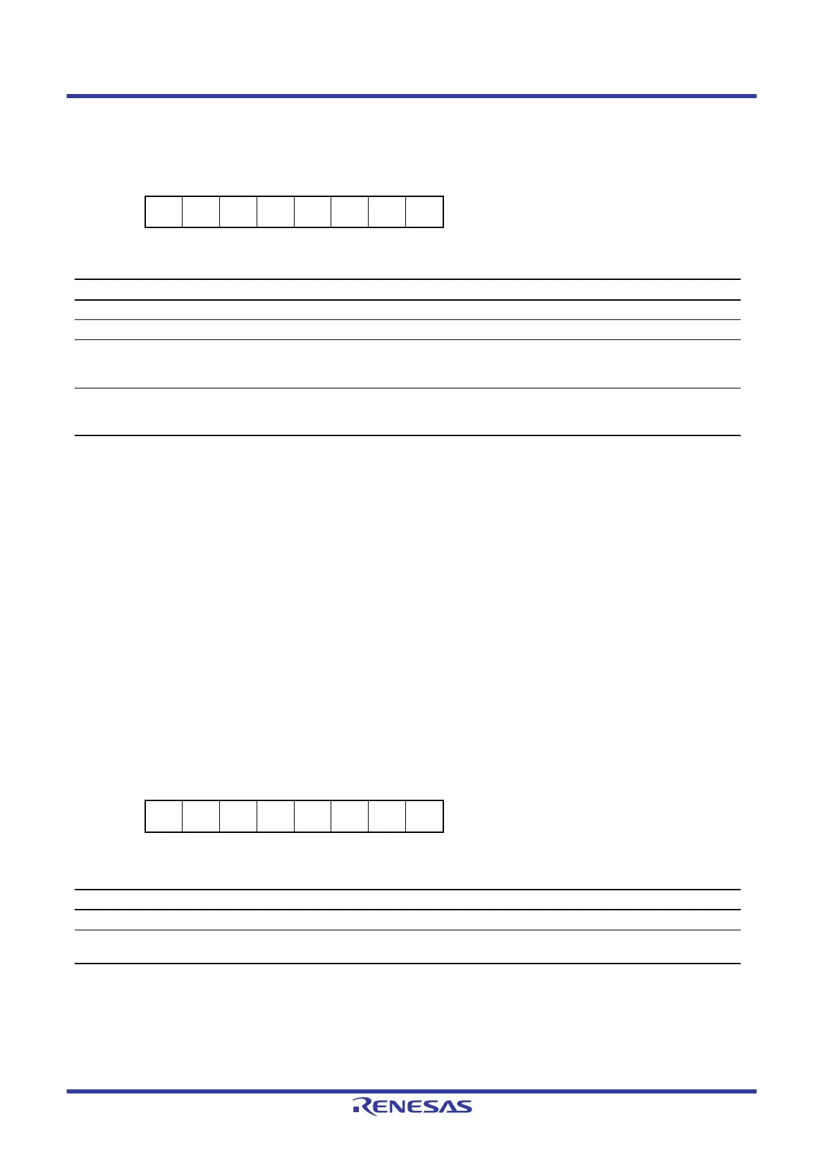
Address(es): DA.DADPR 0008 8045h
b7 b6 b5 b4 b3 b2 b1 b0
DPSEL———————
Value after reset:
00000000
Bit Symbol Bit Name Description R/W
b6 to b0 — Reserved These bits are read as 0. The write value should be 0. R/W
b7 DPSEL Format Select 0: Data is right-justified.
1: Data is left-justified.
R/W

 Loading...


