R01UH0823EJ0100 Rev.1.00 Page 1359 of 1823
Jul 31, 2019
RX23W Group 38. Serial Peripheral Interface (RSPIa)
38.3.2 Controlling RSPI Pins
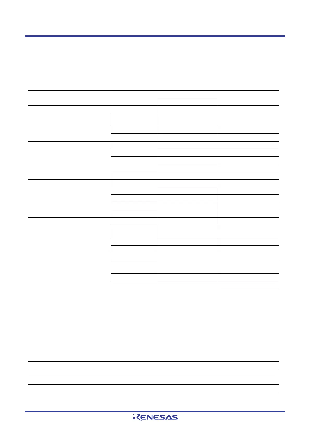
According to the MSTR, MODFEN, and SPMS bits in SPCR and the ODRn.Bi bit for I/O ports, the RSPI can switch pin
states.
Table 38.6 lists the relationship between pin states and bit settings. Setting the ODRn.Bi bit for an I/O port to 0
selects CMOS output; setting it to 1 selects open-drain output. The I/O port settings should follow this relationship.
Note 1. This function is not supported in this mode.
Note 2. RSPI settings are not reflected in the multiplex pins for which the RSPI function is not selected.
Note 3. When SSLA0 is at the active level, the pin state is Hi-Z.
Note 4. When SSLA0 is at the non-active level or the SPCR.SPE bit is 0, the pin state is Hi-Z.
Note 5. These pins are available for use as I/O port pins.
The RSPI in single-master mode (SPI operation) or multi-master mode (SPI operation) determines MOSI signal values
during the SSL negation period (including the SSL retention period during a burst transfer) according to MOIFE and
MOIFV bit settings in SPPCR, as listed in
Table 38.7.
Table 38.6 Relationship between Pin States and Bit Settings
Mode Pin
Pin State*
2
ODRn.Bi Bit for I/O Ports = 0 ODRn.Bi Bit for I/O Ports = 1
Single-master mode (SPI operation)
(MSTR = 1, MODFEN = 0, SPMS = 0)
RSPCKA CMOS output Open-drain output
SSLA0 , SSLA1,
SSLA3
CMOS output Open-drain output
MOSIA CMOS output Open-drain output
MISOA Input Input
Multi-master mode (SPI operation)
(MSTR = 1, MODFEN = 1, SPMS = 0)
RSPCKA*
3
CMOS output/Hi-Z Open-drain output/Hi-Z
SSLA0 Input Input
SSLA1, SSLA3*
3
CMOS output/Hi-Z Open-drain output/Hi-Z
MOSIA*
3
CMOS output/Hi-Z Open-drain output/Hi-Z
MISOA Input Input
Slave mode (SPI operation)
(MSTR = 0, SPMS = 0)
RSPCKA Input Input
SSLA0 Input Input
SSLA1, SSLA3*
5
Hi-Z*
1
Hi-Z*
1
MOSIA Input Input
MISOA*
4
CMOS output/Hi-Z Open-drain output/Hi-Z
Master mode
(Clock synchronous operation)
(MSTR = 1, MODFEN = 0, SPMS = 1)
RSPCKA CMOS output Open-drain output
SSLA0, SSLA1,
SSLA3*
5
Hi-Z*
1
Hi-Z*
1
MOSIA CMOS output Open-drain output
MISOA Input Input
Slave mode
(Clock synchronous operation)
(MSTR = 0, SPMS = 1)
RSPCKA Input Input
SSLA0, SSLA1,
SSLA3*
5
Hi-Z*
1
Hi-Z*
1
MOSIA Input Input
MISOA CMOS output Open-drain output
Table 38.7 MOSI Signal Value Determination during SSL Negation Period
MOIFE Bit MOIFV Bit MOSIA Signal Value during SSL Negation Period
0 0, 1 Final data from previous transfer
1 0 Low
11High

 Loading...


