R01UH0823EJ0100 Rev.1.00 Page 808 of 1823
Jul 31, 2019
RX23W Group 29. Low-Power Timer (LPT)
29.2 Register Descriptions
29.2.1 Low-Power Timer Control Register 1 (LPTCR1)
Note: Set the PRCR.PRC2 bit to 1 (write enabled) before rewriting this register.
Note 1. Satisfy that the frequency of the system clock (ICLK) and peripheral module clock (PCLKB) ≥ 4 × (the frequency of the clock
source).
Note 2. A clock generated by the IWDT-dedicated on-chip oscillator (IWDTCLK) is supplied to the low-power timer. When modifying this
bit, make sure that the IWDT-dedicated on-chip oscillator is oscillating stably.
When the IWDTCLK is used as the clock source for the low-power timer, set the OFS0.IWDTSLCSTP bit to 0 (counting stop is
disabled) in IWDT auto-start mode operation, and set the IWDTCSTPR.SLCSTP bit to 0 (count stop is disabled) in other modes.
Without this setting, the IWDT-dedicated on-chip oscillator is stopped in software standby mode.
The LPTCR1 register is used to control the low-power timer.
LPCNTPSSEL[2:0] Bit (Clock Division Ratio Select)
These bits are used to select the division ratio of the clock source for the low-power timer.
Modify these bits while the LPTCR2.LPCNTSTP bit is 1 (supply of clock to the low-power timer is stopped).
Do not write to these bits while the LPTCR2.LPCNTSTP bit is 0 (clock is supplied to the low-power timer).
LPCNTCKSEL Bit (Clock Source Select)
This bit is used to select the sub-clock or IWDT-dedicated clock as the clock source for the low-power timer.
Modify this bit while the LPTCR2.LPCNTSTP bit is 1 (supply of clock to the low-power timer is stopped).
Do not write to this bit while the LPTCR2.LPCNTSTP bit is 0 (clock is supplied to the low-power timer).
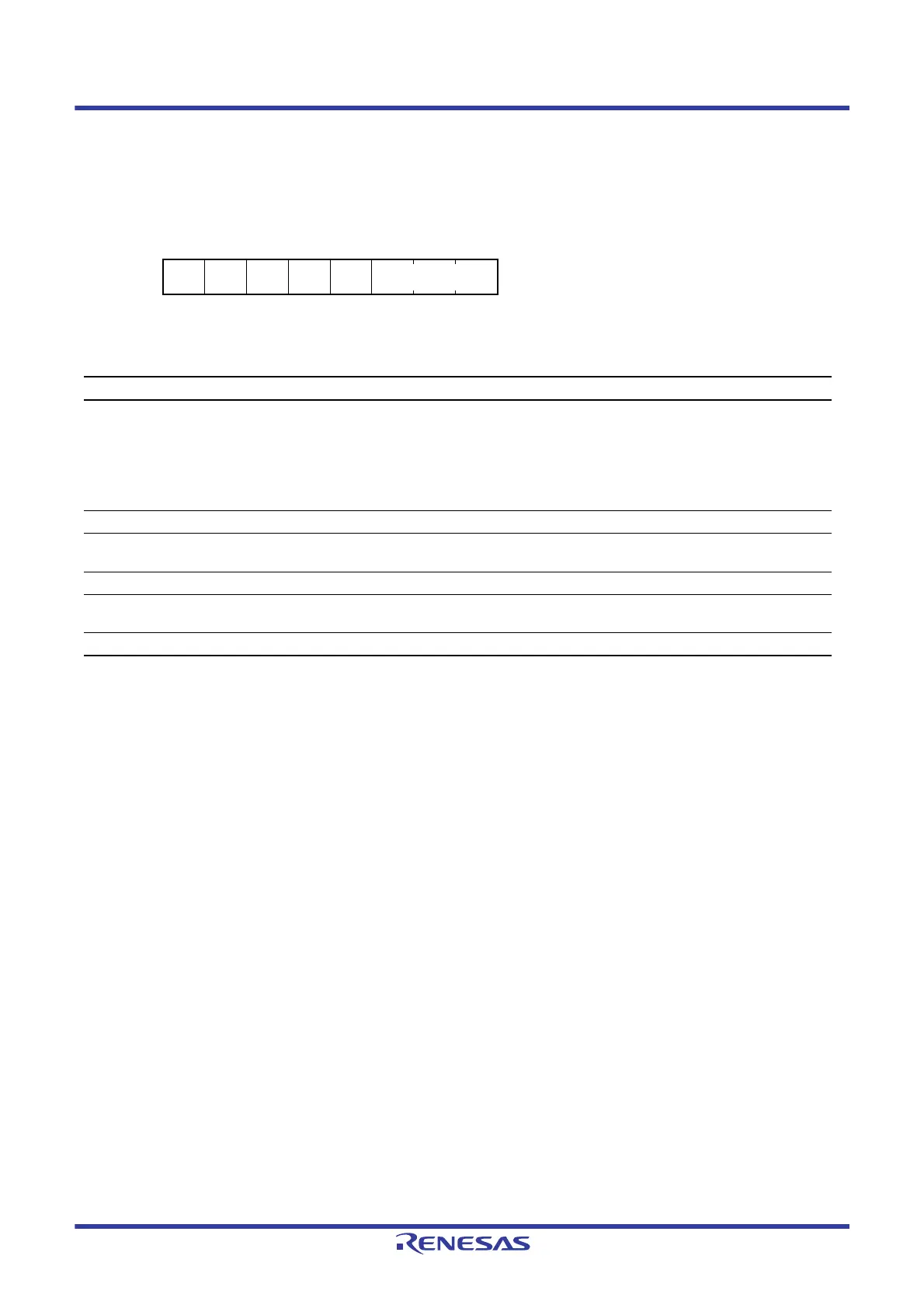
Address(es): LPT.LPTCR1 0008 00B0h
b7 b6 b5 b4 b3 b2 b1 b0
—
LPCMR
E0
—
LPCNT
CKSEL
— LPCNTPSSEL[2:0]
Value after reset:
00000001
Bit Symbol Bit Name Description R/W
b2 to b0 LPCNTPSSEL[2:0] Clock Division Ratio Select
b2 b0
0 0 1: Divided by 2
0 1 0: Divided by 4
0 1 1: Divided by 8
1 0 0: Divided by 16
1 0 1: Divided by 32
Settings other than above are prohibited.
R/W
b3 — Reserved This bit is read as 0. The write value should be 0. R/W
b4 LPCNTCKSEL Clock Source Select*
1
0: Sub-clock
1: IWDT-dedicated clock (IWDTCLK)*
2
R/W
b5 — Reserved This bit is read as 0. The write value should be 0. R/W
b6 LPCMRE0 Compare Match 0 Enable 0: Compare match 0 is disabled
1: Compare match 0 is enabled
R/W
b7 — Reserved This bit is read as 0. The write value should be 0. R/W

 Loading...


