R01UH0823EJ0100 Rev.1.00 Page 1704 of 1823
Jul 31, 2019
RX23W Group 50. Flash Memory (FLASH)
50.8.2 Boot Mode (SCI Interface)
The flash memory can be programmed and erased using asynchronous serial communication in boot mode (SCI
interface). The user area and data area can be rewritten.
When a reset is released while the MD pin and the UB pin are low, the MCU starts in boot mode (SCI interface).
Contact the manufacturer for details on the serial programmer.
50.8.2.1 Operating Conditions in Boot Mode (SCI Interface)
SCI1 is used to communicate with the serial programmer in boot mode (SCI interface).
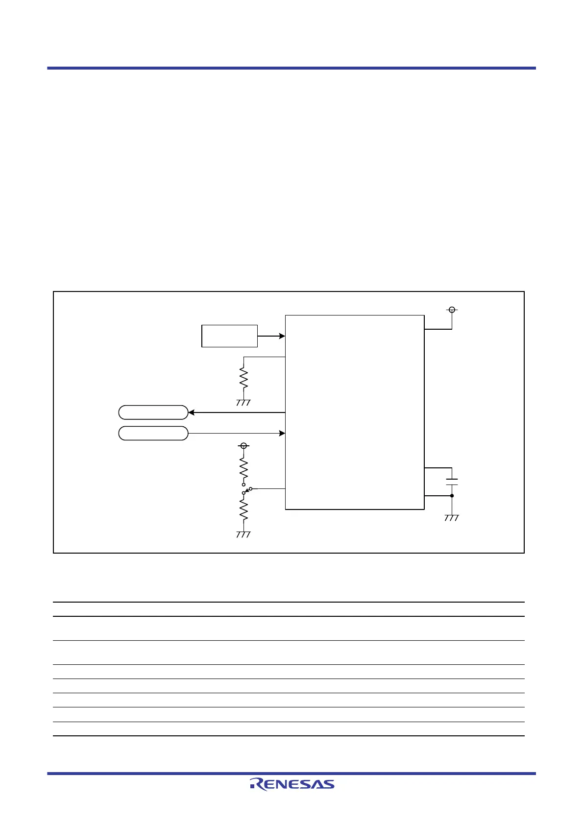
Figure 50.24 shows an Example of Pin Connections in Boot Mode (SCI Interface). Table 50.10 lists Pin Handling in
Boot Mode (SCI Interface).
An example of pin connections shown in
Figure 50.24 is a simplified circuit. Operations are not guaranteed in all
systems.
Figure 50.24 Example of Pin Connections in Boot Mode (SCI Interface)
Table 50.10 Pin Handling in Boot Mode (SCI Interface)
Pin Name Name I/O Function
VCC, VSS Power supply — Input 1.8 V or higher to the VCC pin.
Input 0 V to the VSS pin.
VCL Decoupling capacitor connect
pin
— Connect to the VSS pin via a decoupling capacitor for stabilizing
the internal voltage.
MD Operating mode control Input Input low.
PC7/UB Operating mode control Input Input low.*
1
RES# Reset input Input Reset pin. Connect to the reset circuit.
P30/RXD1 Data input RXD Input Input pin for serial data
P26/TXD1 Data output TXD Output Output pin for serial data
Note 1. Maintain the input level for 2 ms or longer after a reset is released.
MCU
VCC
RES#
UB
TXD1
RXD1
VCL
MD
VSS
Reset circuit
(User logic)
Data input
Data output

 Loading...


