R01UH0823EJ0100 Rev.1.00 Page 1806 of 1823
Jul 31, 2019
RX23W Group 51. Electrical Characteristics
Note: These characteristics apply when noise is not superimposed on the power supply.
Note 1. When OFS1.(LVDAS, FASTSTUP) = 11b.
Note 2. When OFS1.(LVDAS, FASTSTUP) ≠ 11b.
Note 3. The minimum VCC down time indicates the time when VCC is below the minimum value of voltage detection levels V
POR
, V
det0
,
and V
det1
for the POR/LVD.
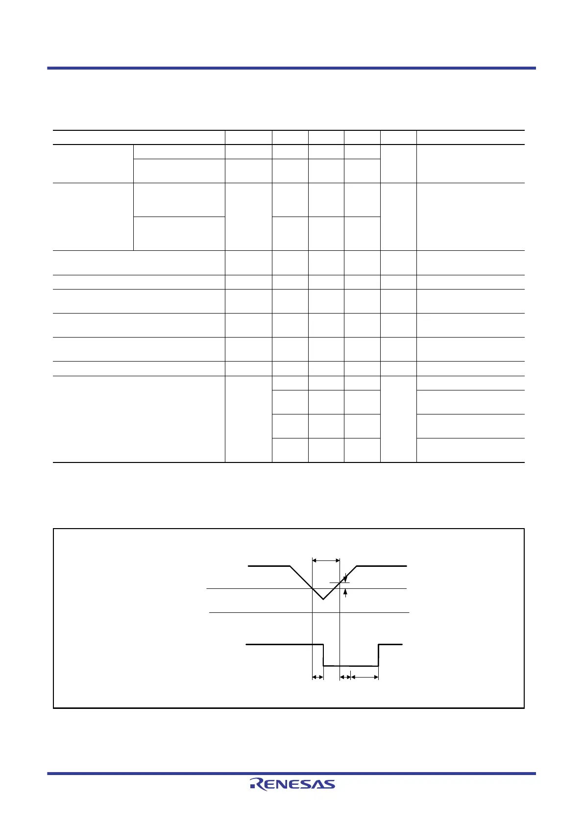
Figure 51.63 Voltage Detection Reset Timing
Table 51.52 Characteristics of Power-On Reset Circuit and Voltage Detection Circuit (2)
Conditions: 1.8 V ≤ VCC0 = VCC_USB = AVCC0 = VCC_RF = AVCC_RF ≤ 3.6 V, VSS = AVSS0 = VSS_USB = VSS_RF = 0 V,
T
a
= –40 to +85°C
Item Symbol Min. Typ. Max. Unit Test Conditions
Wait time after
power-on reset
cancellation
At normal startup*
1
t
POR
― 9.1 ― ms Figure 51.64
During fast startup
time*
2
t
POR
―1.6―
Wait time after
voltage monitoring 0
reset cancellation
Power-on voltage
monitoring 0 reset
disabled*
1
t
LVD0
― 568 ― μs Figure 51.65
Power-on voltage
monitoring 0 reset
enabled*
2
― 100 ―
Wait time after voltage monitoring 1 reset
cancellation
t
LVD1
― 100 ― μs Figure 51.66
Response delay time t
det
― ― 350 μs Figure 51.63
Minimum VCC down time*
3
t
VOFF
350 ― ― μs Figure 51.63, VCC = 1.0 V or
above
Power-on reset enable time t
W(POR)
1 ― ― ms Figure 51.64, VCC = below
1.0 V
LVD operation stabilization time (after LVD is
enabled)
Td
(E-A)
― ― 300 μs Figure 51.66
Hysteresis width (power-on rest (POR)) V
PORH
―110―mV
Hysteresis width (voltage detection circuit:
LVD1)
V
LVH
― 70 ― mV When Vdet1_4 is selected
― 60 ― When Vdet1_5 to Vdet1_9 is
selected
― 50 ― When Vdet1_A or Vdet1_B is
selected
― 40 ― When Vdet1_C or Vdet1_D is
selected
Internal reset signal
(active-low)
VCC
t
VOFF
t
POR
t
det
V
POR
t
det
1.0V
V
PORH

 Loading...


