R01UH0823EJ0100 Rev.1.00 Page 1779 of 1823
Jul 31, 2019
RX23W Group 51. Electrical Characteristics
Note 1. t
Pcyc
: PCLK cycle
Note 2. t
cac
: CAC count clock source cycle
Note 3. When the LOCO is selected as the clock output source (the CKOCR.CKOSEL[2:0] bits are 000b), set the clock output division ratio
selection to divided by 2 (the CKOCR.CKODIV[2:0] bits are 001b).
Note 4. When the EXTAL external clock input or an oscillator is used with divided by 1 (the CKOCR.CKOSEL[2:0] bits are 010b and the
CKOCR.CKODIV[2:0] bits are 000b) to output from CLKOUT, the above should be satisfied with an input duty cycle of 45 to 55%.
Note 5. The voltage for VCC_RF when CLKOUT_RF pin is to be used is between 3.0 V and 3.6 V.
CLKOUT_RF
*5
CLKOUT_RF pin output cycle t
CRFcyc
250 — ns Figure 51.43
CLKOUT_RF pin high pulse width t
CRFH
100 — ns
CLKOUT_RF pin low pulse width t
CRFL
100 — ns
CLKOUT_RF pin output rise time t
CRFr
—5ns
CLKOUT_RF pin output fall time t
CRFf
—5ns
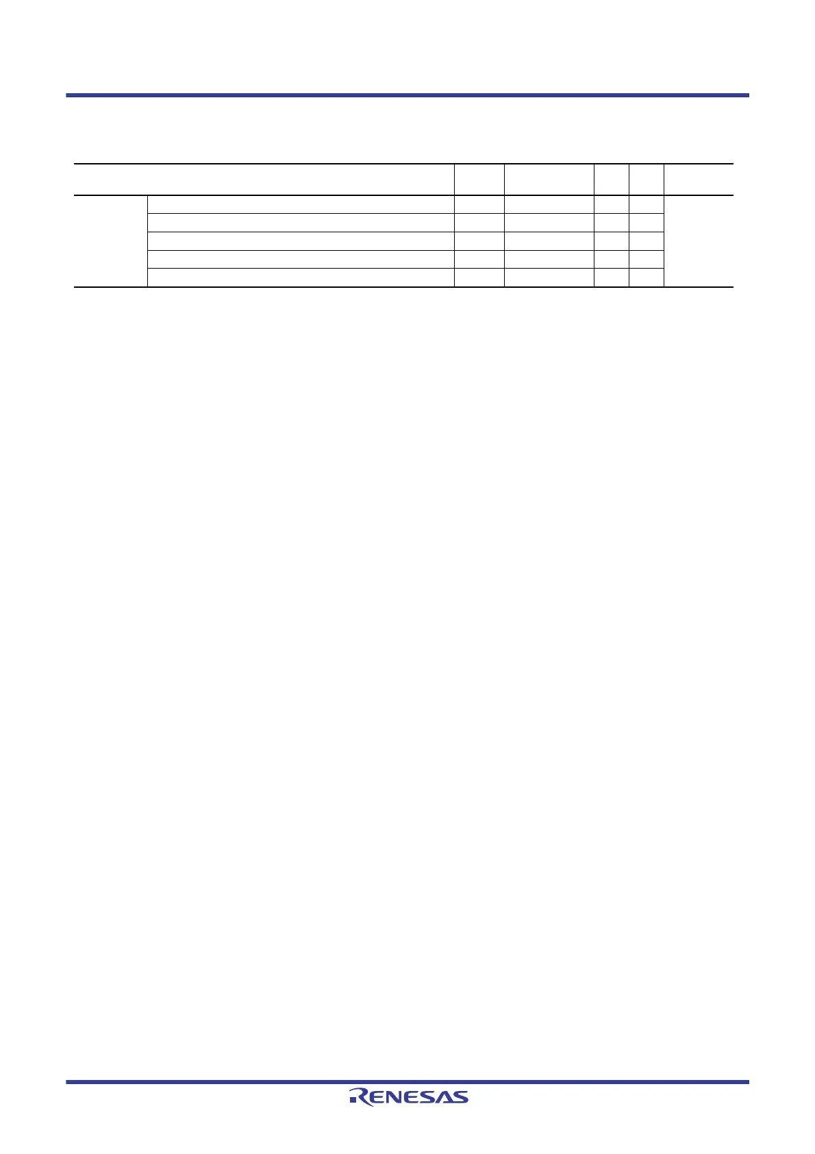
Table 51.32 Timing of On-Chip Peripheral Modules (1)
Conditions: 1.8 V ≤ VCC = VCC_USB = AVCC0 = VCC_RF = AVCC_RF ≤ 3.6 V, VSS = AVSS0 = VSS_USB = VSS_RF = 0 V,
T
a
= –40 to +85°C
Item Symbol Min. Max.
Unit
*1
Test
Conditions

 Loading...


