R01UH0823EJ0100 Rev.1.00 Page 1780 of 1823
Jul 31, 2019
RX23W Group 51. Electrical Characteristics
Note 1. t
Pcyc
: PCLK cycle
Note 2. N: An integer from 1 to 8 that can be set by the RSPI clock delay register (SPCKD)
Note 3. N: An integer from 1 to 8 that can be set by the RSPI slave select negation delay register (SSLND)
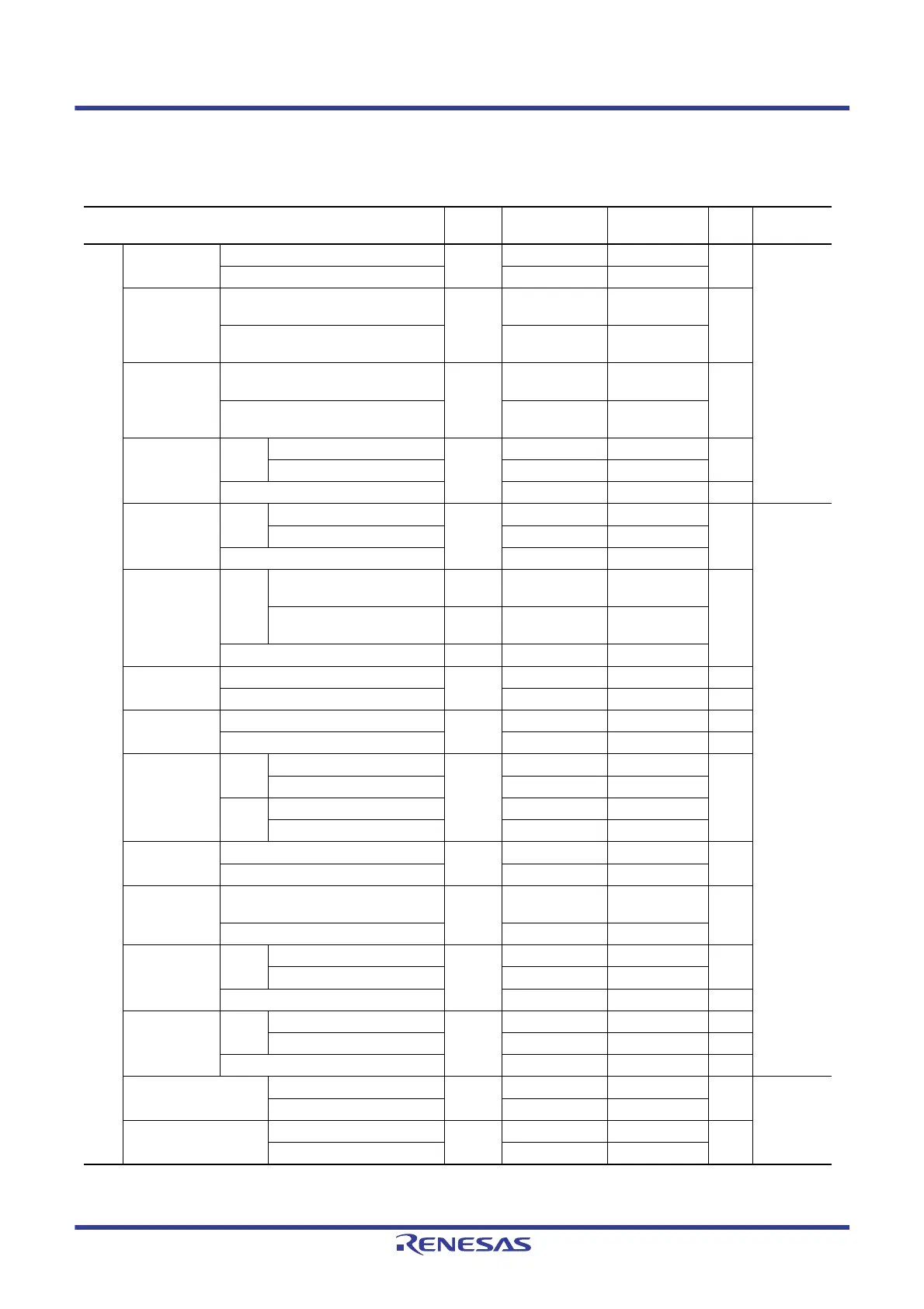
Table 51.33 Timing of On-Chip Peripheral Modules (2)
Conditions: 1.8 V ≤ VCC = VCC_USB = AVCC0 = VCC_RF = AVCC_RF ≤ 3.6 V, VSS = AVSS0 = VSS_USB = VSS_RF = 0 V,
T
a
= –40 to +85°C, C = 30 pF, when high-drive output is selected by the drive capacity control register
Item Symbol Min. Max. Unit
Test
Conditions
RSPI RSPCK clock
cycle
Master t
SPcyc
2 4096 t
Pcyc
*
1
Figure 51.44
Slave 8 4096
RSPCK clock
high pulse width
Master t
SPCKWH
(t
SPcyc
– t
SPCKr
–
t
SPCKf
)/2 – 3
—ns
Slave (t
SPcyc
– t
SPCKr
–
t
SPCKf
)/2
—
RSPCK clock
low pulse width
Master t
SPCKWL
(t
SPcyc
– t
SPCKr
–
t
SPCKf
)/2 – 3
—ns
Slave (t
SPcyc
– t
SPCKr
–
t
SPCKf
)/2
—
RSPCK clock
rise/fall time
Output 2.7 V or above t
SPCKr
,
t
SPCKf
—10ns
1.8 V or above — 15
Input — 1 μs
Data input setup
time
Master 2.7 V or above t
SU
10 — ns Figure 51.45
to
Figure 51.48
1.8 V or above 30 —
Slave 25 – t
Pcyc
—
Data input hold
time
Master RSPCK set to a division ratio
other than PCLKB divided by 2
t
H
t
Pcyc
—ns
RSPCK set to PCLKB divided
by 2
t
HF
0—
Slave t
H
20 + 2 × t
Pcyc
—
SSL setup time Master t
LEAD
–30 + N*
2
× t
SPcyc
—ns
Slave 2 — t
Pcyc
SSL hold time Master t
LAG
–30 + N*
3
× t
SPcyc
—ns
Slave 2 — t
Pcyc
Data output
delay time
Master 2.7 V or above t
OD
—14ns
1.8 V or above — 30
Slave 2.7 V or above — 3 × t
Pcyc
+ 65
1.8 V or above — 3 × t
Pcyc
+105
Data output hold
time
Master t
OH
0—ns
Slave 0 —
Successive
transmission
delay time
Master t
TD
t
SPcyc
+ 2 × t
Pcyc
8 × t
SPcyc
+ 2 ×
t
Pcyc
ns
Slave 4 × t
Pcyc
—
MOSI and MISO
rise/fall time
Output 2.7 V or above t
Dr
, t
Df
—10ns
1.8 V or above — 15
Input — 1 μs
SSL rise/fall
time
Output 2.7 V or above t
SSLr
,
t
SSLf
—10ns
1.8 V or above — 15 ns
Input — 1 μs
Slave access time 2.7 V or above t
SA
—6t
Pcyc
Figure 51.47,
Figure 51.48
1.8 V or above — 7
Slave output release
time
2.7 V or above t
REL
—5t
Pcyc
1.8 V or above — 6

 Loading...


