R01UH0823EJ0100 Rev.1.00 Page 1781 of 1823
Jul 31, 2019
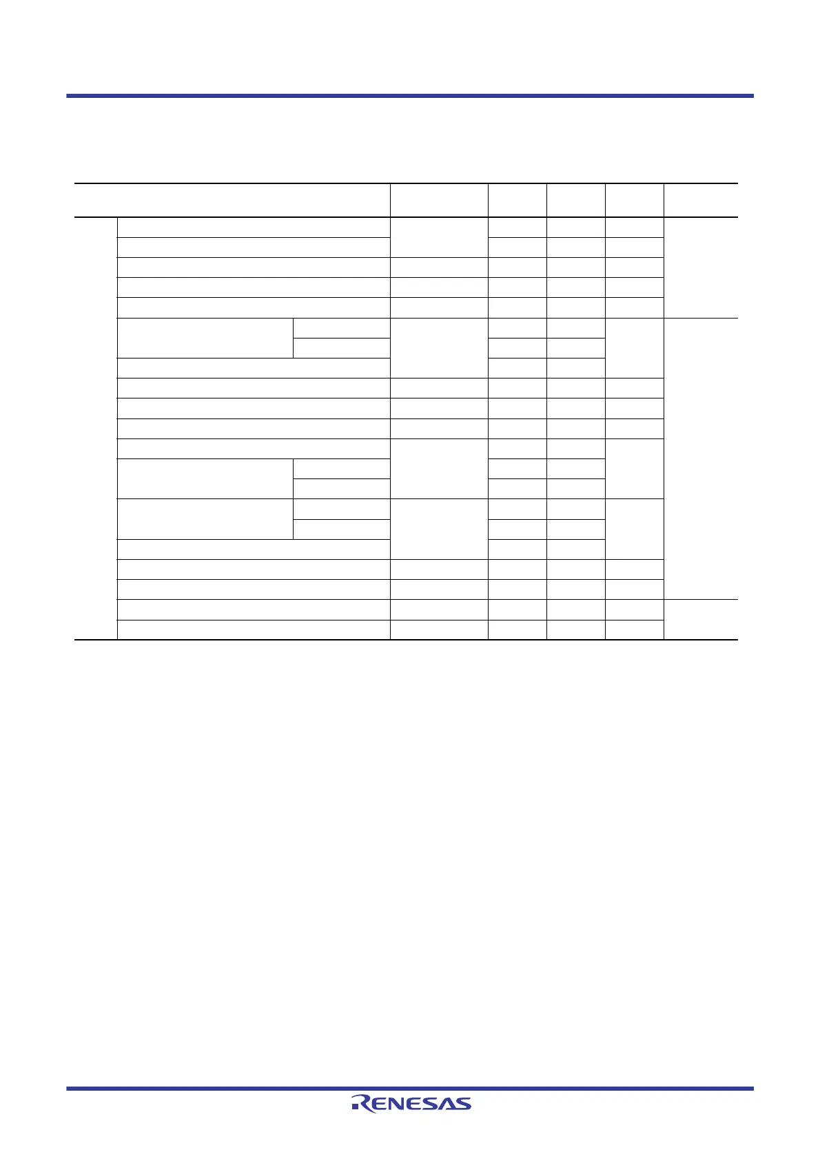
RX23W Group 51. Electrical Characteristics
Note 1. t
Pcyc
: PCLK cycle
Table 51.34 Timing of On-Chip Peripheral Modules (3)
Conditions: 1.8 V ≤ VCC = VCC_USB = AVCC0 = VCC_RF = AVCC_RF ≤ 3.6 V, VSS = AVSS0 = VSS_USB = VSS_RF = 0 V,
T
a
= –40 to +85°C
Item Symbol Min. Max. Unit*
1
Test
Conditions
Simple
SPI
SCK clock cycle output (master) t
SPcyc
4 65536 t
Pcyc
Figure 51.44
SCK clock cycle input (slave) 6 65536 t
Pcyc
SCK clock high pulse width t
SPCKWH
0.4 0.6 t
SPcyc
SCK clock low pulse width t
SPCKWL
0.4 0.6 t
SPcyc
SCK clock rise/fall time t
SPCKr
, t
SPCKf
—20ns
Data input setup time (master) 2.7 V or above t
SU
65 — ns Figure 51.45,
Figure 51.46
1.8 V or above 95 —
Data input setup time (slave) 40 —
Data input hold time t
H
40 — ns
SSL input setup time t
LEAD
3—t
SPcyc
SSL input hold time t
LAG
3—t
SPcyc
Data output delay time (master) t
OD
—40ns
Data output delay time (slave) 2.7 V or above — 65
1.8 V or above — 100
Data output hold time (master) 2.7 V or above t
OH
–10 — ns
1.8 V or above –20 —
Data output hold time (slave) –10 —
Data rise/fall time t
Dr
, t
Df
—20ns
SSL input rise/fall time t
SSLr
, t
SSLf
—20ns
Slave access time t
SA
—6t
Pcyc
Figure 51.47,
Figure 51.48
Slave output release time t
REL
—6t
Pcyc

 Loading...


