R01UH0823EJ0100 Rev.1.00 Page 1788 of 1823
Jul 31, 2019
RX23W Group 51. Electrical Characteristics
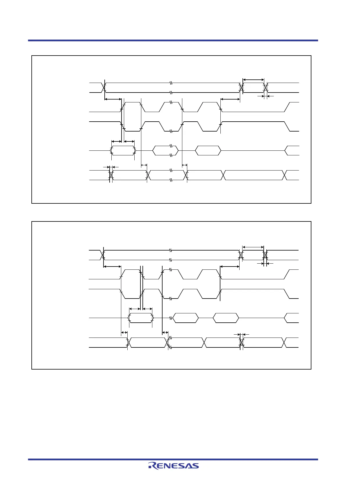
Figure 51.45 RSPI Timing (Master, CPHA = 0) and Simple SPI Clock Timing (Master, CKPH = 1)
Figure 51.46 RSPI Timing (Master, CPHA = 1) and Simple SPI Clock Timing (Master, CKPH = 0)
t
Dr,
t
Df
t
SU
t
H
t
LEAD
t
TD
t
LAG
t
SSLr,
t
SSLf
t
OH
t
OD
MSB IN DATA LSB IN MSB IN
MSB OUT DATA LSB OUT IDLE MSB OUT
SCKn
CKPOL = 0
output
SCKn
CKPOL = 1
output
SMISOn
input
SMOSIn
output
Simple SPIRSPI
SSLA0 to
SSLA3
output
RSPCKA
CPOL = 0
output
RSPCKA
CPOL = 1
output
MISOA
input
MOSIA
output
SSLA0 to
SSLA3
output
RSPCKA
CPOL = 0
output
RSPCKA
CPOL = 1
output
MISOA
input
MOSIA
output
RSPI
Simple SPI
SCKn
CKPOL = 1
output
SCKn
CKPOL = 0
output
SMISOn
input
SMOSIn
output
t
Dr,
t
Df
t
SU
t
H
t
LEAD
t
TD
t
LAG
t
SSLr,
t
SSLf
t
OH
MSB IN DATA LSB IN MSB IN
MSB OUT DATA LSB OUT IDLE MSB OUT
t
OD

 Loading...


