R01UH0823EJ0100 Rev.1.00 Page 1782 of 1823
Jul 31, 2019
RX23W Group 51. Electrical Characteristics
Note: t
IICcyc
: RIIC internal reference clock (IICφ) cycle
Note 1. The value in parentheses is used when the ICMR3.NF[1:0] bits are set to 11b while a digital filter is enabled with the ICFER.NFE
bit = 1.
Note 2. C
b
is the total capacitance of the bus lines.
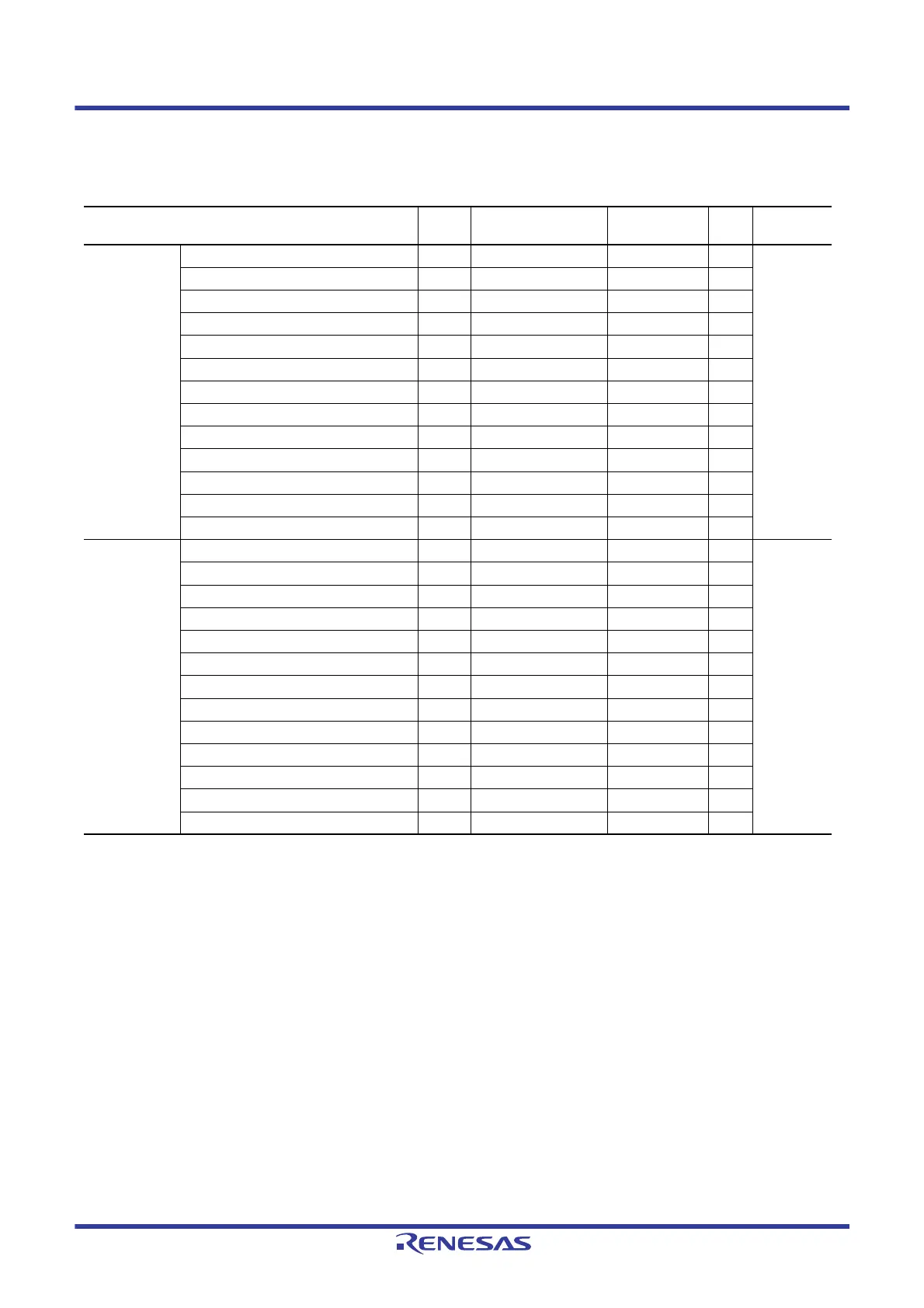
Table 51.35 Timing of On-Chip Peripheral Modules (4)
Conditions: 2.7 V ≤ VCC = VCC_USB = AVCC0 = VCC_RF = AVCC_RF ≤ 3.6 V, VSS = AVSS0 = VSS_USB = VSS_RF = 0 V,
fPCLKB ≤ 32 MHz, T
a
= –40 to +85°C
Item Symbol Min.*
1,
*
2
Max. Unit
Test
Conditions
RIIC
(Standard
mode, SMBus)
SCL cycle time t
SCL
6 (12) × t
IICcyc
+ 1300 — ns Figure 51.49
SCL high pulse width t
SCLH
3 (6) × t
IICcyc
+ 300 — ns
SCL low pulse width t
SCLL
3 (6) × t
IICcyc
+ 300 — ns
SCL, SDA rise time t
Sr
— 1000 ns
SCL, SDA fall time t
Sf
— 300 ns
SCL, SDA spike pulse removal time t
SP
0 1 (4) × t
IICcyc
ns
SDA bus free time t
BUF
3 (6) × t
IICcyc
+ 300 — ns
START condition hold time t
STAH
t
IICcyc
+ 300 — ns
Repeated START condition setup time t
STAS
1000 — ns
STOP condition setup time t
STOS
1000 — ns
Data setup time t
SDAS
t
IICcyc
+ 50 — ns
Data hold time t
SDAH
0—ns
SCL, SDA capacitive load C
b
— 400 pF
RIIC
(Fast mode)
SCL cycle time t
SCL
6 (12) × t
IICcyc
+ 600 — ns Figure 51.49
SCL high pulse width t
SCLH
3 (6) × t
IICcyc
+ 300 — ns
SCL low pulse width t
SCLL
3 (6) × t
IICcyc
+ 300 — ns
SCL, SDA rise time t
Sr
— 300 ns
SCL, SDA fall time t
Sf
— 300 ns
SCL, SDA spike pulse removal time t
SP
0 1 (4) × t
IICcyc
ns
SDA bus free time t
BUF
3 (6) × t
IICcyc
+ 300 — ns
START condition hold time t
STAH
t
IICcyc
+ 300 — ns
Repeated START condition setup time t
STAS
300 — ns
STOP condition setup time t
STOS
300 — ns
Data setup time t
SDAS
t
IICcyc
+ 50 — ns
Data hold time t
SDAH
0—ns
SCL, SDA capacitive load C
b
— 400 pF

 Loading...


