R01UH0823EJ0100 Rev.1.00 Page 1783 of 1823
Jul 31, 2019
RX23W Group 51. Electrical Characteristics
Note: t
Pcyc
: PCLK cycle
Note 1. C
b
is the total capacitance of the bus lines.
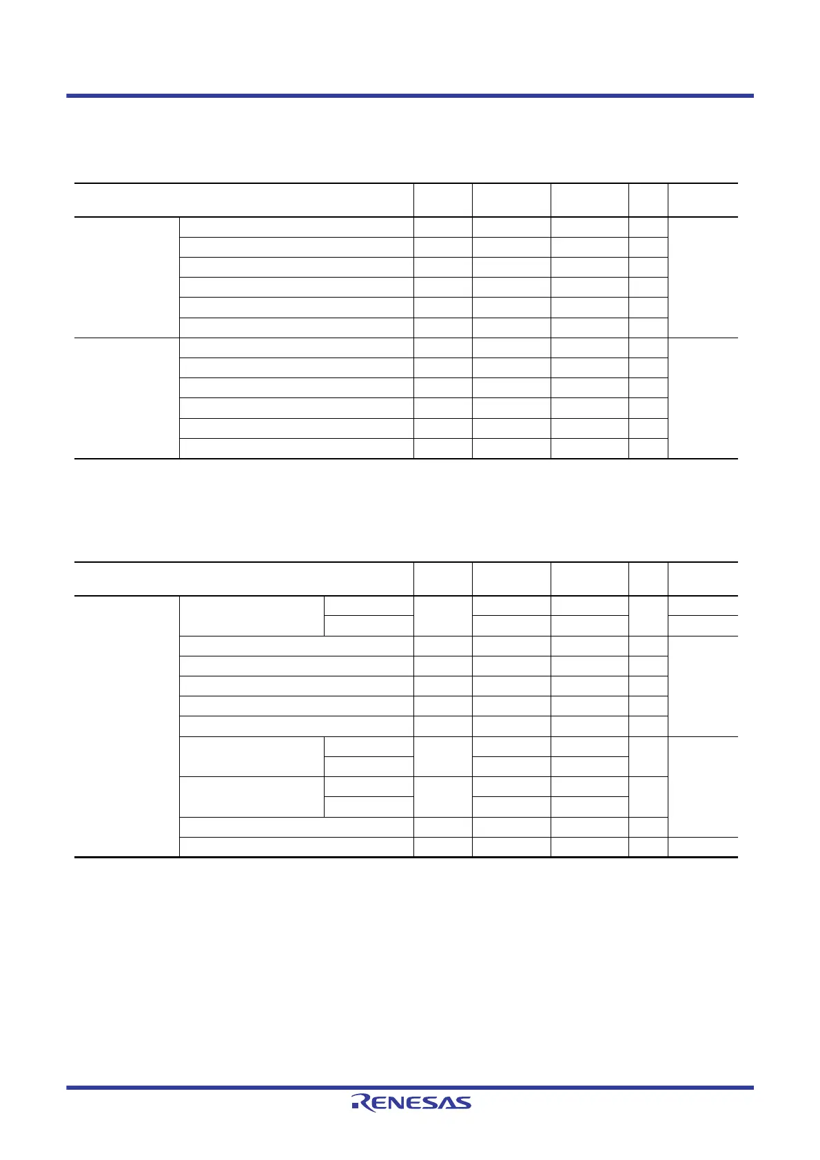
Table 51.36 Timing of On-Chip Peripheral Modules (5)
Conditions: 2.7 V ≤ VCC = VCC_USB = AVCC0 = VCC_RF = AVCC_RF ≤ 3.6 V, VSS = AVSS0 = VSS_USB = VSS_RF = 0 V,
fPCLKB ≤ 32 MHz, T
a
= –40 to +85°C
Item Symbol Min.*
1
Max. Unit
Test
Conditions
Simple I
2
C
(Standard mode)
SSDA rise time t
Sr
— 1000 ns Figure 51.49
SSDA fall time t
Sf
— 300 ns
SSDA spike pulse removal time t
SP
0 4 × t
Pcyc
ns
Data setup time t
SDAS
250 — ns
Data hold time t
SDAH
0—ns
SSCL, SSDA capacitive load C
b
— 400 pF
Simple I
2
C
(Fast mode)
SSDA rise time t
Sr
— 300 ns Figure 51.49
SSDA fall time t
Sf
— 300 ns
SSDA spike pulse removal time t
SP
0 4 × t
Pcyc
ns
Data setup time t
SDAS
100 — ns
Data hold time t
SDAH
0—ns
SSCL, SSDA capacitive load C
b
— 400 pF
Table 51.37 Timing of On-Chip Peripheral Modules (6)
Conditions: 1.8 V ≤ VCC = VCC_USB = AVCC0 = VCC_RF = AVCC_RF ≤ 3.6 V, VSS = AVSS0 = VSS_USB = VSS_RF = 0 V,
fPCLKB ≤ 32 MHz, T
a
= –40 to +85°C
Item Symbol Min. Max. Unit
Test
Conditions
SSI AUDIO_MCLK input
frequency
2.7 V or above t
AUDIO
125MHz
1.8 V or above 1 4
Output clock cycle t
O
250 — ns Figure 51.50
Input clock cycle t
I
250 — ns
Clock high level t
HC
0.4 0.6 to, ti
Clock low level t
LC
0.4 0.6 to, ti
Clock rise time t
RC
—20ns
Data delay time 2.7 V or above t
DTR
— 65 ns Figure 51.51
Figure 51.52
1.8 V or above — 105
Setup time 2.7 V or above t
SR
65 — ns
1.8 V or above 90 —
Hold time t
HTR
40 — ns
WS changing edge SSIDATA output delay t
DTRW
— 105 ns Figure 51.53

 Loading...


