R01UH0823EJ0100 Rev.1.00 Page 1784 of 1823
Jul 31, 2019
RX23W Group 51. Electrical Characteristics
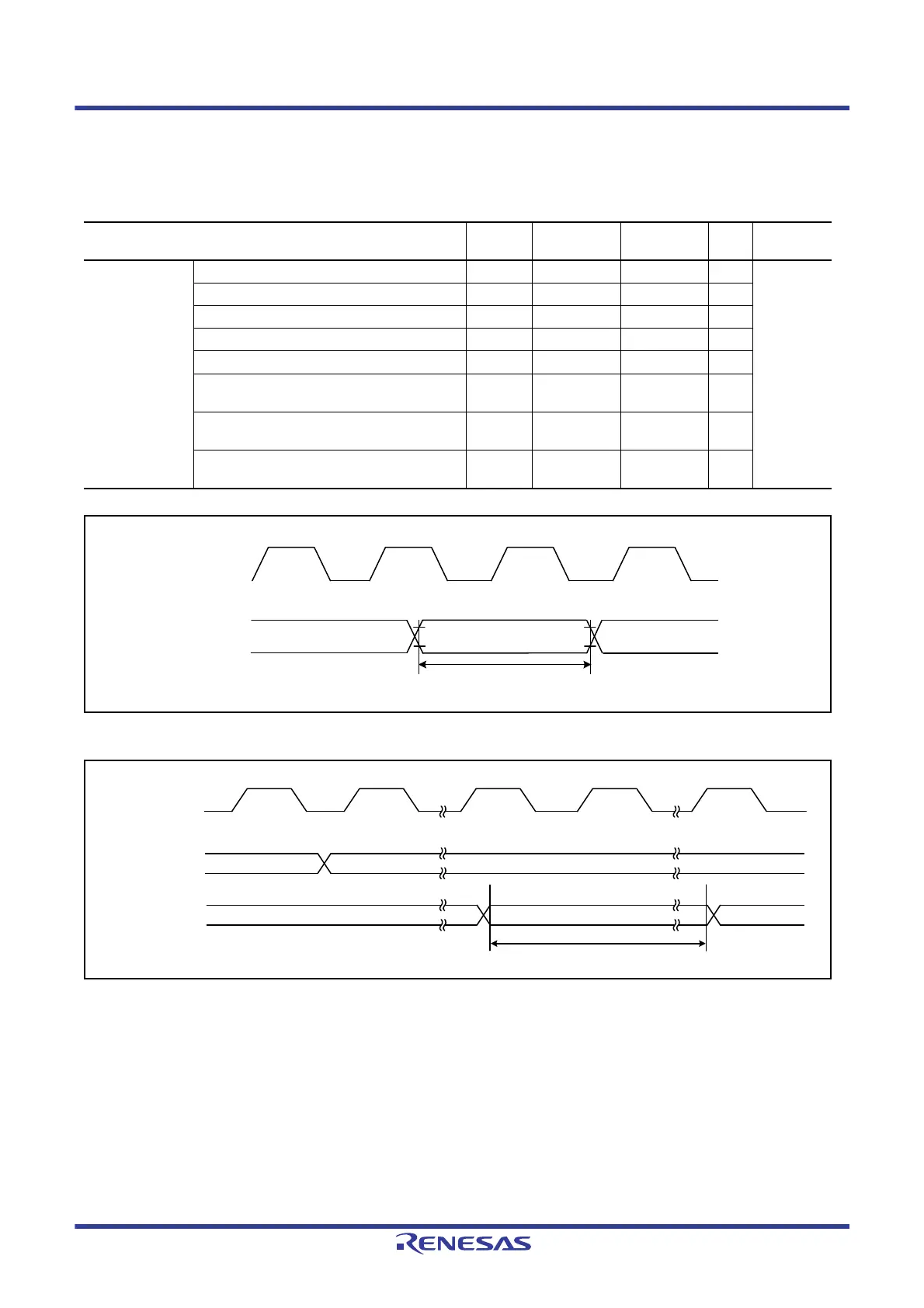
Figure 51.34 I/O Port Input Timing
Figure 51.35 MTU Input/Output Timing
Table 51.38 Timing of On-Chip Peripheral Modules (7)
Conditions: 2.7 V ≤ VCC = VCC_USB = AVCC0 = VCC_RF = AVCC_RF ≤ 3.6 V, VSS = AVSS0 = VSS_USB = VSS_RF = 0 V,
fPCLKB ≤ 32 MHz, T
a
= –40 to +85°C,
when high-drive output is selected by the drive capacity control register
Item Symbol Min. Max. Unit
Test
Conditions
SDHI SDHI_CLK pin output cycle time t
PP(SD)
62.5 — ns Figure 51.54
SDHI_CLK pin output high pulse width t
WH(SD)
18.25 — ns
SDHI_CLK pin output low pulse width t
WL(SD)
18.25 — ns
SDHI_CLK pin output rise time t
TLH(SD)
—10ns
SDHI_CLK pin output fall time t
THL(SD)
—10ns
Output data delay time (data transfer mode) for
SDHI_CMD and SDHI_D0 to SDHI_D3 pins
t
ODLY(SD)
–18.25 18.25 ns
Input data setup time for SDHI_CMD and
SDHI_D0 to SDHI_D3 pins
t
ISU(SD)
9.25 — ns
Input data hold time for SDHI_CMD and
SDHI_D0 to SDHI_D3 pins
t
IH(SD)
8.3 — ns
Output
compare output
Input capture
input
PCLK
t
TICW

 Loading...


