R01UH0823EJ0100 Rev.1.00 Page 1811 of 1823
Jul 31, 2019
RX23W Group 51. Electrical Characteristics
Note: The time until each operation of the flash memory is started after instructions are executed by software is not included.
Note: The lower-limit frequency of FCLK is 1 MHz during programming or erasing of the flash memory. When using FCLK at below
4 MHz, the frequency can be set to 1 MHz, 2 MHz, or 3 MHz. A non-integer frequency such as 1.5 MHz cannot be set.
Note: The frequency accuracy of FCLK must be within ±3.5%.
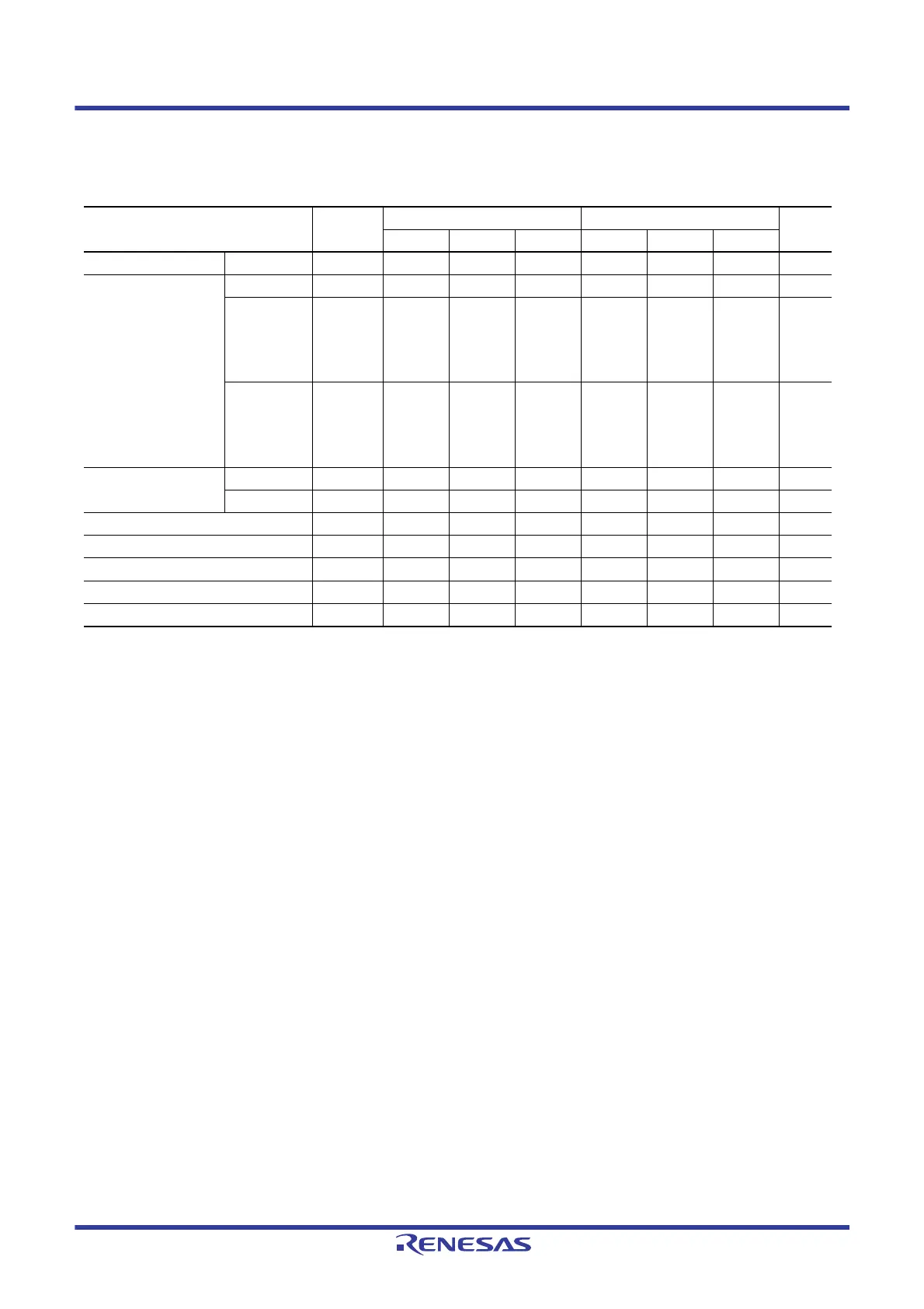
Table 51.57 ROM (Flash Memory for Code Storage) Characteristics (3) Middle-Speed Operating Mode
Conditions: 1.8 V ≤ VCC = VCC_USB = AVCC0 = VCC_RF = AVCC_RF ≤ 3.6 V, VSS = AVSS0 = VSS_USB= VSS_RF = 0 V
Temperature range for the programming/erasure operation: T
a
= –40 to +85°C
Item Symbol
FCLK = 1 MHz FCLK = 8 MHz
Unit
Min. Typ. Max. Min. Typ. Max.
Programming time 8-byte t
P8
— 152 1367 — 97.9 936 μs
Erasure time 2-Kbyte t
E2K
— 8.8 279.7 — 5.9 221 ms
512-Kbyte
(when block
erase
command is
used)
t
E512K
— 928 19221 — 191 4108 ms
512-Kbyte
(when all-
block erase
command is
used)
t
EA512K
— 923 19015 — 185 3901 ms
Blank check time 8-byte t
BC8
— — 85.0 — — 50.88 μs
2-Kbyte t
BC2K
— — 1870 — — 402 μs
Erase operation forced stop time t
SED
— — 28.0 — — 21.3 μs
Start-up area switching setting time t
SAS
— 13.0 573.3 — 7.7 451 ms
Access window time t
AWS
— 13.0 573.3 — 7.7 451 ms
ROM mode transition wait time 1 t
DIS
2.0 — — 2.0 — — μs
ROM mode transition wait time 2 t
MS
3.0 — — 3.0 — — μs

 Loading...


