SDRAM Controller
3-42 ADSP-21368 SHARC Processor Hardware Reference
SDRAM power-up mode.
SDPM bit 11. If the SDPM bit is set (=1), the SDC
does a precharge all command, followed by a load mode register com-
mand, and eight auto-refresh cycles. If the SDPM bit is cleared (=0), the
SDC does a precharge all command, followed by eight auto-refresh cycles,
and a load mode register command.
SDRAM bank column address width. SDCAW bits 13–12 shown in
Table 3-16. Sets the SDRAM page size. Page sizes of 256 and 512 bits,
and 1K and 2K bits are supported. Table 3-22 on page 3-53 shows the
page size and breakdown of the internal address (IA31–0), as seen from the
core into the row, bank, and column address. The column address makes
up the address inside the page.
[
Programming the SDC with non-supported page size values pro-
duces unpredictable results.
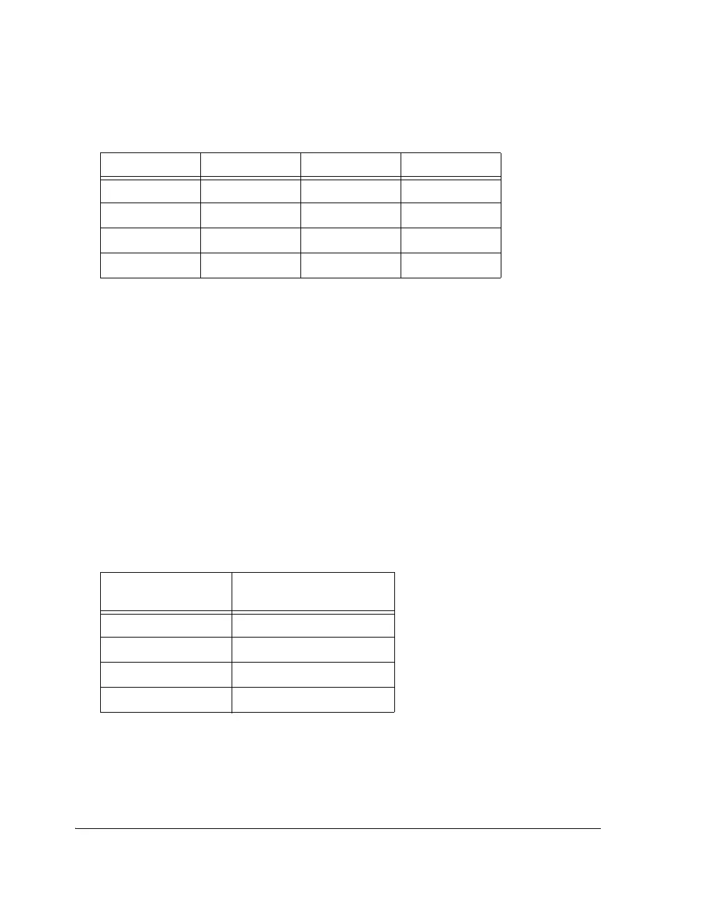
Table 3-15. Precharge Delay Bit Settings
Bit Setting Clock Cycles Bit Setting Clock Cycles
000 Reserved SDTRP4 = 100 4
SDTRP1 = 001 1 SDTRP5 = 101 5
SDTRP2 = 010 2 SDTRP6 = 110 6
SDTRP3 = 011 3 SDTRP7 = 111 7
Table 3-16. SDRAM Bank Column Address Width Bit Settings
SDCAW Bit Setting SDRAM Bank Column
Address Width
SDCAW8 = 00 8 bits (256 words)
SDCAW9 = 01 9 bits (512 words)
SDCAW10 = 10 10 bits (1K words)
SDCAW11 = 11 11 bits (2K words)
 Loading...


