ADSP-21368 SHARC Processor Hardware Reference 3-53
External Port
lines are decoded memory address lines that change at the same time as the
other address lines. When no external memory access is occurring, the
MS3-0 lines are inactive.
The width of the bank address is only two bits and is shown in
Table 3-21. The width of the column address is programmable. The row
address is also programmable using SDRAW bits. The SDRAM bank address
is calculated using the row address width and the column address width.
In the following sections and in Table 3-22 through Table 3-25, the map-
ping of internal addresses to the external addresses is discussed. The
mapping of the addresses depends on the row address width (SDRAW), col-
umn address width (SDCAW), and the X16DE bit setting.
In Table 3-22, X16DE = 0, SDRAW[2:0] = 100 (12 bits), and SDCAW[1:0]
= 10 (10 bits).
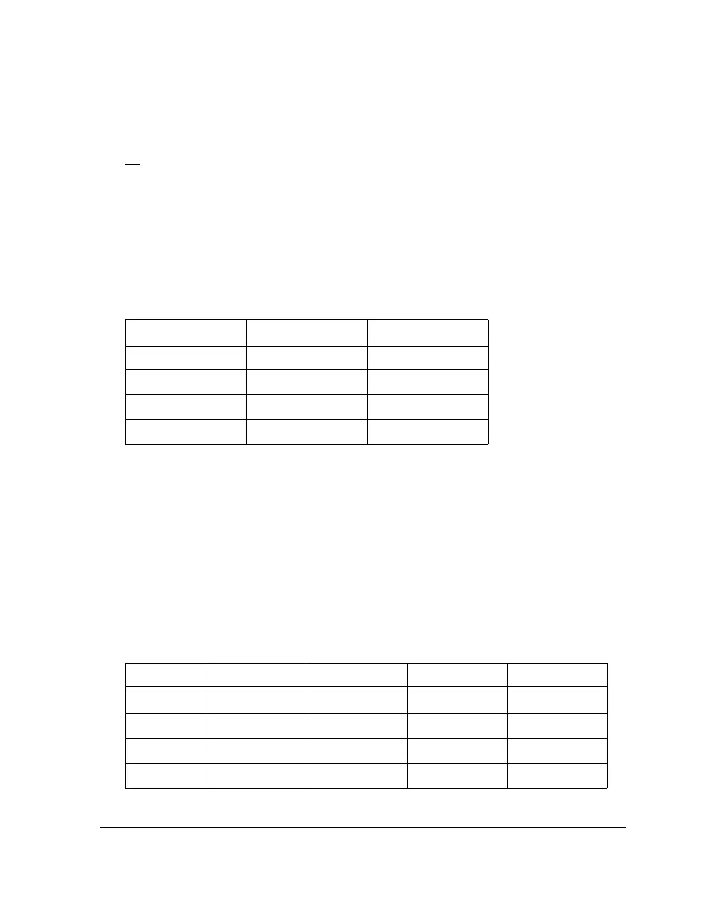
Table 3-21. External Memory Address Bank Decoding
IA[27] IA[26] External Bank
00Bank 0
01Bank 1
10Bank 2
11Bank 3
Table 3-22. 32-Bit Column, Row, and Bank Address Mapping
(1K Words)
Pin Column Address Row Address Bank Address Pins of SDRAM
A[18] IA[23] BA[1]
A[17] IA[22] BA[0]
A[13] A[12]
A[12] IA[21] A[11]
 Loading...


