SDRAM Controller
3-52 ADSP-21368 SHARC Processor Hardware Reference
On the ADSP-21367/8/9 and ADSP-2137x processors, bank 0 starts at
address 0x20 0000 in external memory and is followed in order by banks
1, 2, and 3. When the processor generates an address located within one of
the four banks, it asserts the corresponding memory select line,
MS3-0.
The external memory address ranges are shown in Table 3-20.
L
External memory address space is supported in normal word
addressing mode only. Single-instruction, multiple-data (SIMD),
extended-precision, short word, and long word addressing modes
are not supported. Program execution from external memory is also
not supported in the ADSP-21367/8/9 processors but is supported
in the ADSP-2137x processors. For more information, “External
Memory Interface on the ADSP-2137x Processors” on page 3-3.
The
MS3-0 outputs serve as chip selects for memories or other external
devices, eliminating the need for external decoding logic. For more infor-
mation, see “Timing External Memory Accesses” on page 3-36. The
MS3-0
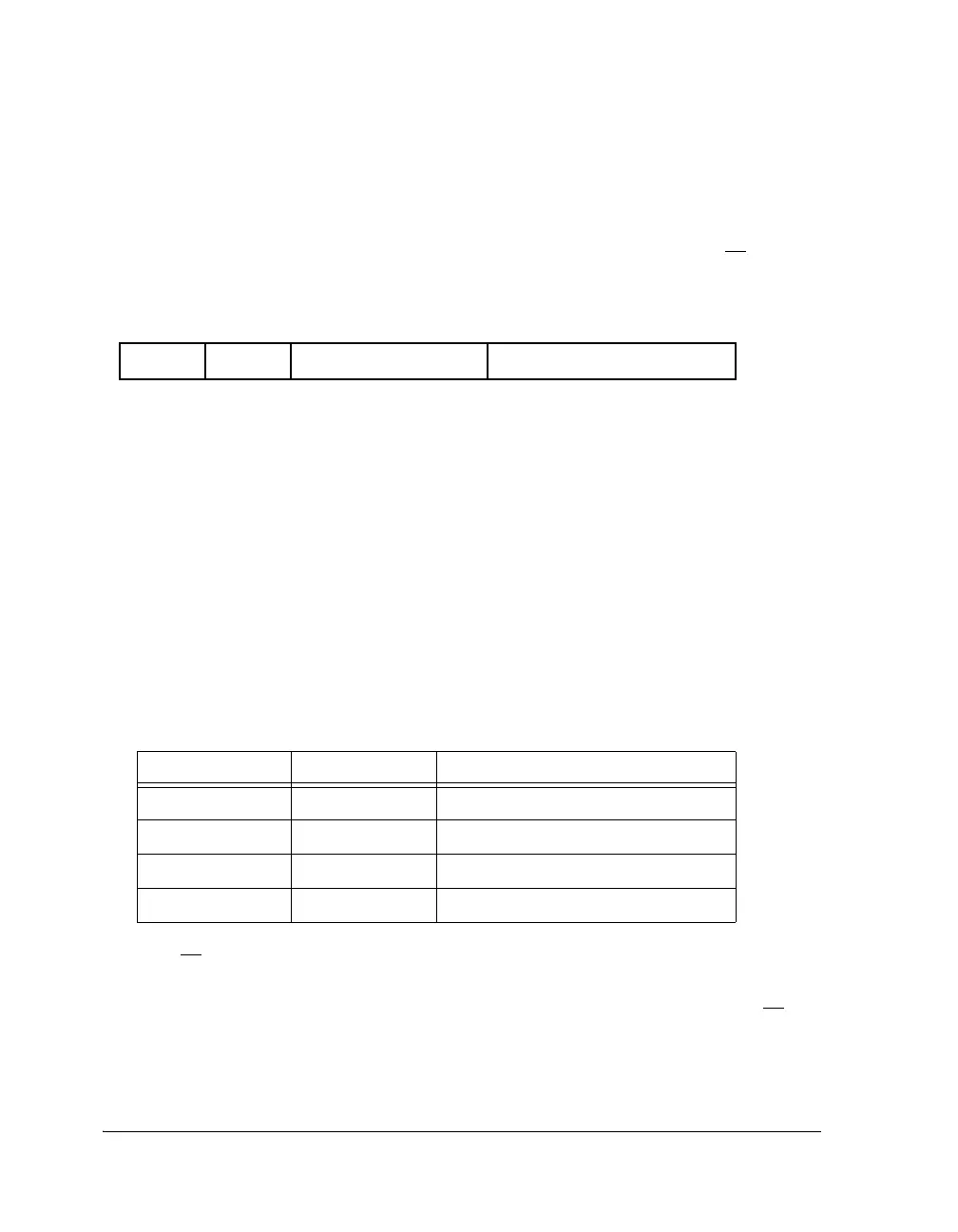
Figure 3-8. Core Address Mapping to Bank, Row, and Column Addresses
Table 3-20. External Memory Address Space for SDRAM Addresses
Bank Size in Words Address Range
Bank 0 62M 0x0020 0000 – 0x03FF FFFF
Bank 1 64M 0x0400 0000 – 0x07FF FFFF
Bank 2 64M 0x0800 0000 – 0x0BFF FFFF
Bank 3 64M 0x0C00 0000 – 0x0FFF FFFF
31 0
Unused
Bank
Column AddressRow Address
Address
 Loading...


