EasyManuals Logo

Renesas RX Series User Manual

Renesas RX Series
1823 pages
To Next Page IconTo Next Page
To Previous Page IconTo Previous Page
Page #102 background imageLoading...
Page #102 background image
R01UH0823EJ0100 Rev.1.00 Page 102 of 1823
Jul 31, 2019
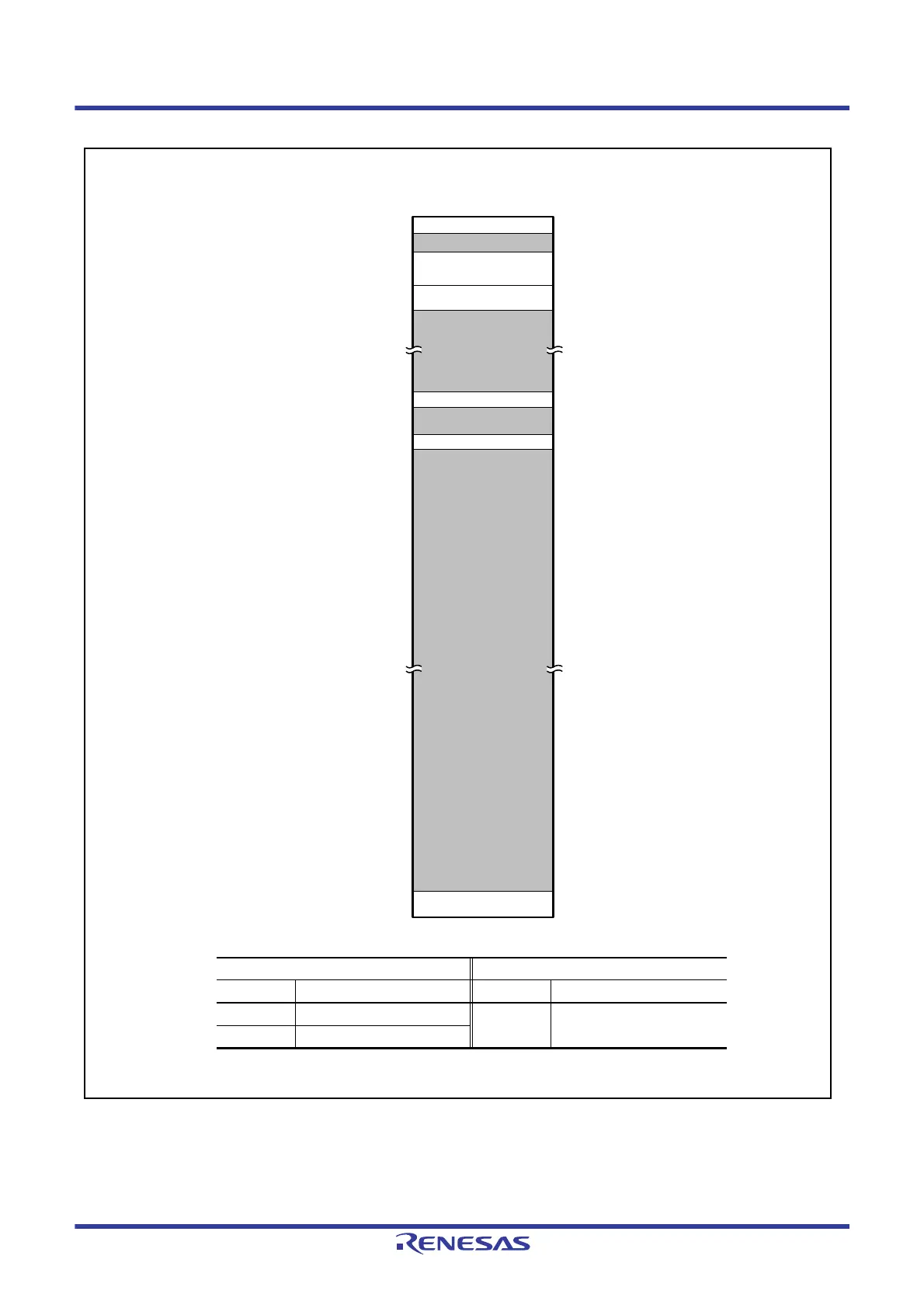
RX23W Group 4. Address Space
Figure 4.1 Memory Map in Each Operating Mode
Reserved area
*3
Reserved area
*3
Reserved area
*3
On-chip ROM (E2 Data Flash)
Reserved area
*3
0000 0000h
0008 0000h
FFFF FFFFh
Single-chip mode
*1
RAM
*2
On-chip ROM (program ROM)
(read only)*
2
0010 0000h
Peripheral I/O registers
0010 2000h
0080 0000h
FFF8 0000h
Peripheral I/O registers
007F C000h
007F C500h
007F FC00h
0001 0000h
Note 1. The capacity of ROM differs depending on the products.
Note: See Table 1.3 List of Products, for the product type name.
ROM (bytes) RAM (bytes)
Capacity Address Capacity Address
512 Kbytes FFF8 0000h to FFFF FFFFh 64 Kbytes 0000 0000h to 0000 FFFFh
384 Kbytes FFFA 0000h to FFFF FFFFh

Table of Contents

Questions and Answers:

Question and Answer IconNeed help?

Do you have a question about the Renesas RX Series and is the answer not in the manual?

Renesas RX Series Specifications

General IconGeneral
CoreRXv1, RXv2, RXv3
Flash MemoryUp to 8 MB
RAMUp to 1 MB
Operating Voltage1.62V to 5.5V
Operating Temperature-40°C to +85°C or +105°C
PackageBGA, LQFP
ADC Resolution12-bit
DAC Resolution12-bit
Communication InterfacesSCI, SPI, I2C, USB, Ethernet, CAN
Architecture32-bit
Security FeaturesMemory Protection Unit (MPU)

Related product manuals