R01UH0823EJ0100 Rev.1.00 Page 1296 of 1823
Jul 31, 2019
RX23W Group 36. CAN Module (RSCAN)
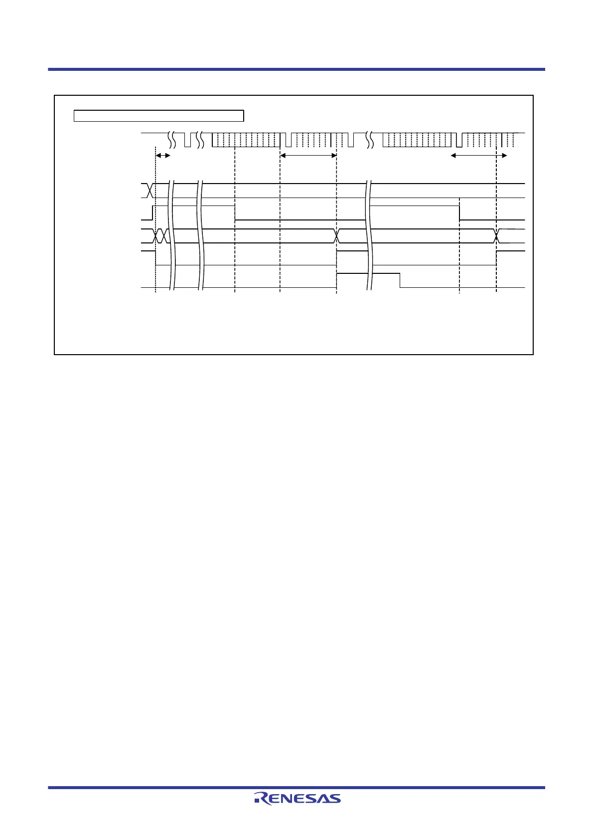
Figure 36.31 Transmit/Receive FIFO Buffer Transmission Timing Chart (Transmit Abort Completed)
(1) While the CAN bus is idle, when the CFCCL0.CFE value is 1 (transmit/receive FIFO buffer 0 is used) and the
CFCCL0.CFDC[2:0] value is 001b (4 messages) or more and the CFSTS0.CFMC[5:0] value is 01h or more, the
priority determination processing starts to determine the highest-priority transmit message. When the highest-
priority transmit message has been determined, transmission of the message starts.
(2) When transmission is in progress or it is determined that the transmit/receive FIFO buffer is used for the next
transmission, message transmission is not aborted unless an error or arbitration lost occurs even if the CFCCL0.CFE
bit is set to 0 (no transmit/receive FIFO buffer 0 is used).
(3) When a transmit request from a buffer is present, the priority determination starts with the CRC delimiter for the
next transmission. In this figure, transmit/receive FIFO buffer 0 is not selected as a buffer for the next transmission.
(4) When transmit completes successfully, the CFSTS0.CFMC[5:0] value becomes 00h. Setting the CFCCL0.CFIM bit
to 1 (a FIFO transmit interrupt request is generated each time a message has been transmitted) sets the
CFSTS0.CFTXIF flag to 1 (a transmit/receive FIFO transmit interrupt request is present). The CFSTS0.CFTXIF
flag can be cleared by the program.
(5) If another CAN node on the CAN bus is transmitting data (not from transmit/receive FIFO buffer 0), transmit/
receive FIFO buffer 0 cannot be disabled immediately even if the CFCCL0.CFE bit is set to 0 (no transmit/receive
FIFO buffer 0 is used) during transmit priority determination. (The CFSTS0.CFEMP flag is not set to 1 (the
transmit/receive FIFO buffer contains no message (buffer empty)) immediately.)
(6) After the internal processing time has passed, transmit/receive FIFO buffers are disabled and the
CFSTS0.CFMC[5:0] flags become 00h and the CFSTS0.CFEMP flag becomes 1. When the transmit/receive FIFO
buffer 0 is not transmitting data and is not selected as the next transmit buffer and priority determination is not in
progress, the transmit/receive FIFO buffer 0 is immediately disabled. (The CFSTS0.CFMC[5:0] flags become 00h
and the CFSTS0.CFEMP flag becomes 1.)
CFDC[2:0], CFE: Bits in the CFCCL0 register
CFMC[5:0], CFEMP, CFTXIF: Flags in the CFSTS0 register
Example of transmission from transmit/receive FIFO buffer 0
SOF
Determine next
transmit priority
Determine next
transmit priority
EOF
SOF
INT
CRC
delimiter
High
Low
[Transmit/receive FIFO buffer 0]
CAN bus
030201
0 1
(1)
(2) (3) (4)
(5) (6)
EOF
INT
CRC
delimiter
Determine next
transmit priority
CFDC[2:0] bits
CFE bit
CFMC[5:0] bits
CFEMP flag
CFTXIF flag
1
0
1
0
1
0

 Loading...


