R01UH0823EJ0100 Rev.1.00 Page 453 of 1823
Jul 31, 2019
RX23W Group 22. Multi-Function Pin Controller (MPC)
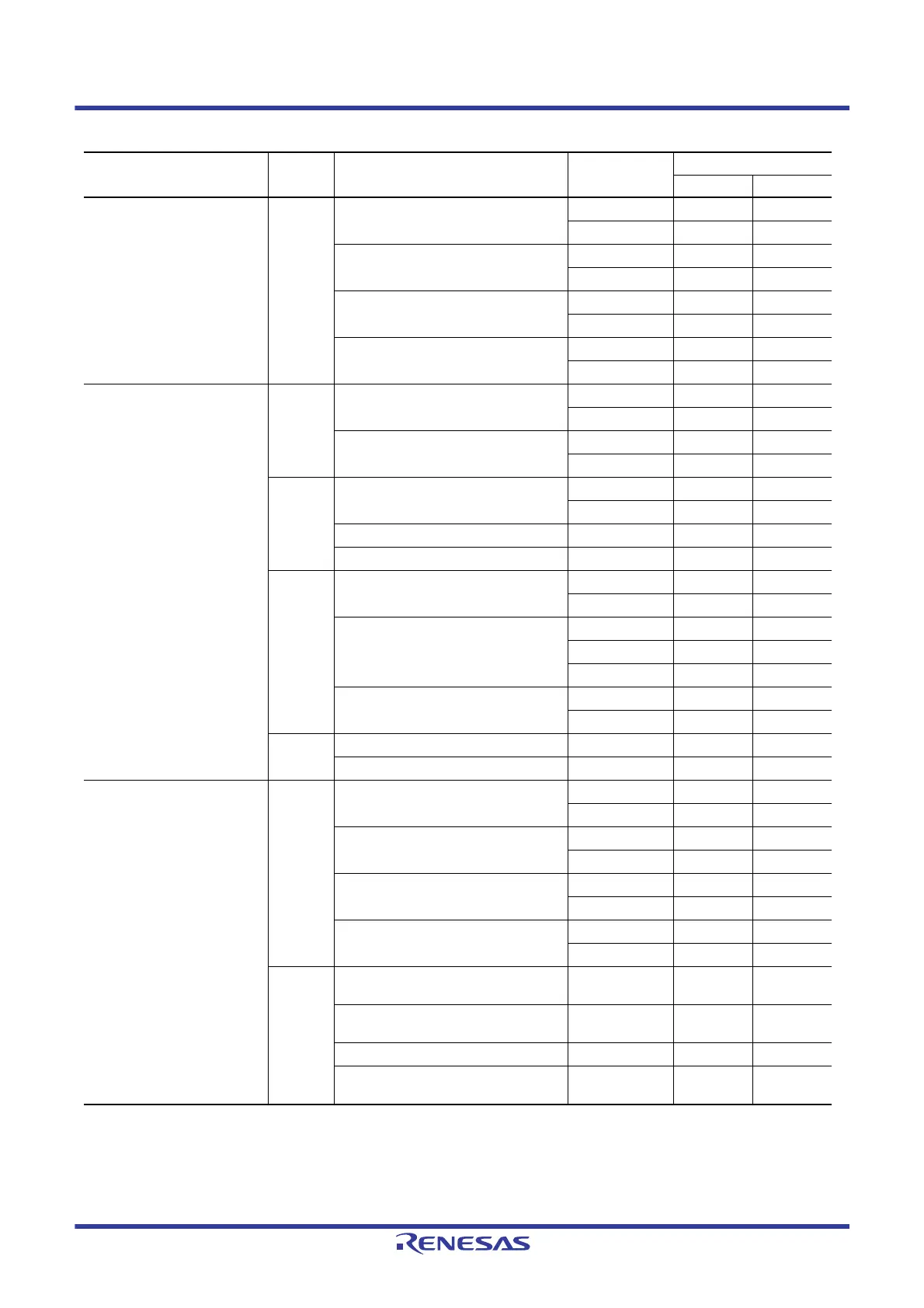
16-bit timer pulse unit TPU TCLKA (input) P14
PC2
TCLKB (input) P15
PC3
TCLKC (input) P16
PC0
TCLKD (input) P17
PB3 ×
8-bit timer TMR0 TMO0 (output) P22
×
PB3
×
TMCI0 (input) P21
×
PB1
TMR1 TMO1 (output) P17
P26
TMCI1 (input) PC4
TMRI1 (input) PB5 ×
TMR2 TMO2 (output) P16
PC7
TMCI2 (input) P15
P31
PC6
TMRI2 (input) P14
PC5
TMR3 TMCI3 (input) P27
TMRI3 (input) P30
Serial communications
interface
SCI1 RXD1 (input)/SMISO1 (input/output)/
SSCL1 (input/output)
P15
P30
TXD1 (output)/SMOSI1 (input/output)/
SSDA1 (input/output)
P16
P26
SCK1 (input/output) P17
P27
CTS1# (input)/RTS1# (output)/SS1#
(input)
P14
P31
SCI5 RXD5 (input)/SMISO5 (input/output)/
SSCL5 (input/output)
PC2
TXD5 (output)/SMOSI5 (input/output)/
SSDA5 (input/output)
PC3
SCK5 (input/output) PC4
CTS5# (input)/RTS5# (output)/SS5#
(input/output)
PC0
Table 22.1 Allocation of Pin Functions to Multiple Pins (3/6)
Module/Function Channel Pin Functions Allocation Port
Package
84-pin 56-pin
 Loading...


