SDRAM Controller
3-44 ADSP-21368 SHARC Processor Hardware Reference
• If cleared (=0), a 32-bit SDRAM should be used;
DATA[31–0] should be connected to the SDRAM data pins;
ADDR[15:1] should be connected SDRAM address pins 14–0. For
more information, see “SDRAM Address Mapping” on page 3-51.
Note that ADDR[18:17] pins are also used. See tables Table 3-22 on
page 3-53 to Table 3-25 on page 3-57 for bank address usage.
SDRAM tWR parameter setting. SDTWR bits 18–17. Defines the required
delay, in number of SDCLK cycles, between the time the SDC issues a write
command (drives write data) and a precharge command.
The t
WR
parameter enables applications to accommodate the SDRAM’s
timing requirements. For more information, see “Timing External Mem-
ory Accesses” on page 3-36. Any value between 1 and 3 SDCLK cycles may
be selected as shown in Table 3-17.
SDRAM optional refresh.
SDORF bit 19. Used for memories built as
SDRAM in FPGAs. When set (=1), auto-refresh is not performed and the
Force AR bit does not have any effect. When cleared (=0), auto-refresh
occurs when the refresh counter expires. See also “SDRAM Refresh Rate
Control Register (SDRRC)” on page 3-49.
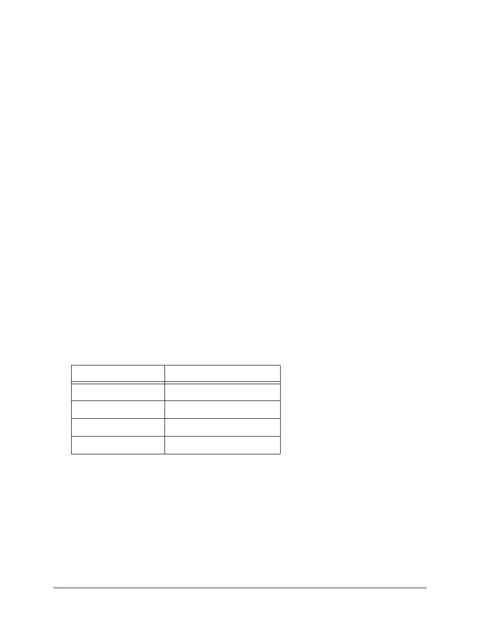
Table 3-17. SDRAM t
WR
Bit Settings
SDTWR Bit Setting SDRAM Parameter Setting
00 Reserved
SDTWR1 = 01 One clock cycle
SDTWR2 = 10 Two clock cycles
SDTWR3 = 11 Three clock cycles
SDTWR
t
WRmin
t
SDCLK
------------------
≥
 Loading...


