SPORT Control Registers and Data Buffers
5-50 ADSP-21368 SHARC Processor Hardware Reference
Table 5-5 through Table 5-8 provides a complete list of the SPORT regis-
ters in IOP address order, showing the memory-mapped IOP address and
a brief description of each register.
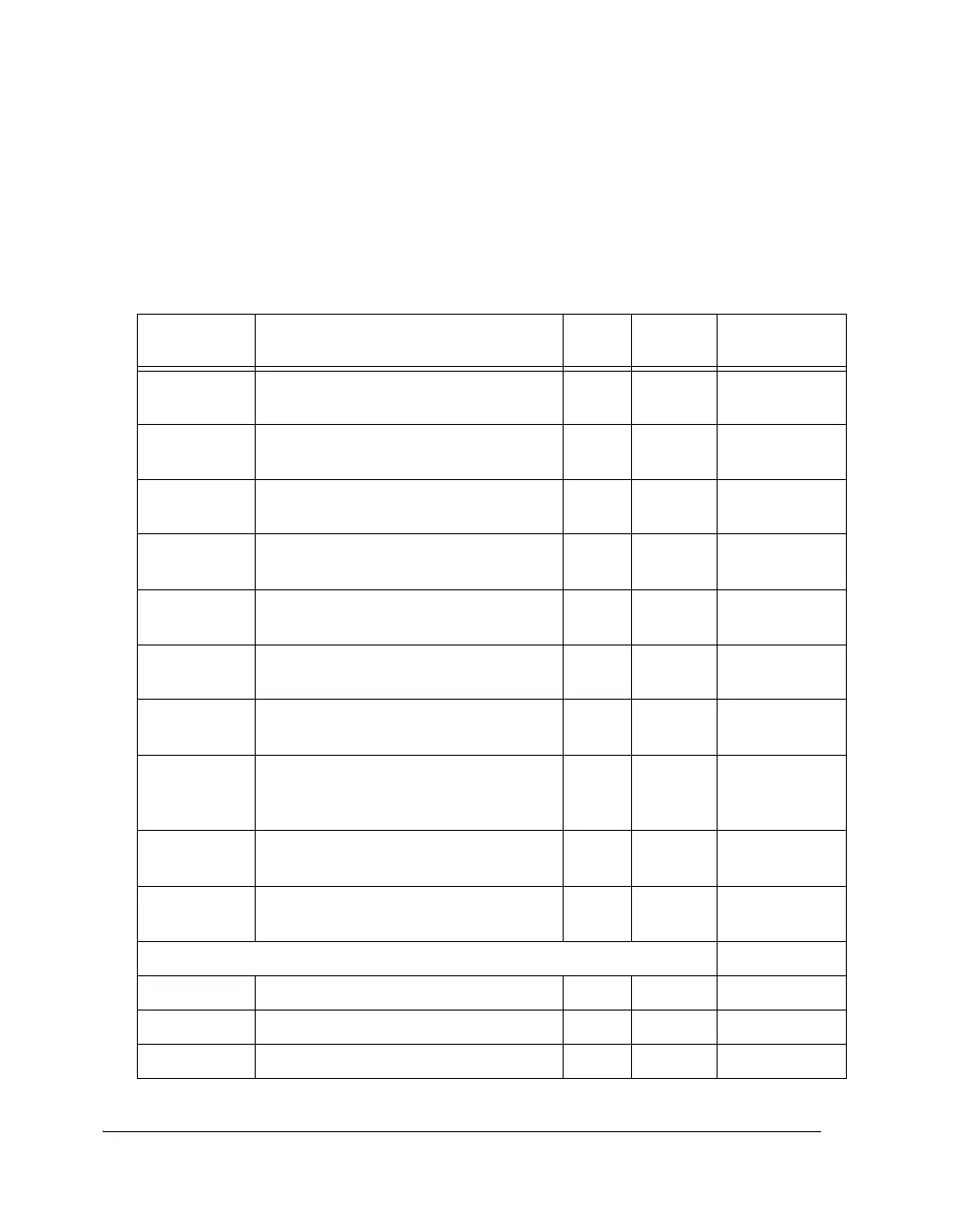
Table 5-5. SPORT0 and SPORT1 Registers
Register
Name
Function Width No. of
Registers
Memory Map
[17:0]
SPCTL0–1 SPORT Control Register for SPORT0,
SPORT1
32 2 00C00–00C01
DIV0–1 Clock and Frame Sync Divisors for
SPORT0, SPORT1
32 2 00C02–00C03
SPMCTL0 SPORT Multichannel Control Register
for SPORT0
32 1 00C04
SP0CS0–3 Multichannel Active channels select for
SPORT0
32 4 00C05–00C08
SP1CS0–3 Multichannel Active channels select for
SPORT1
32 4 00C09–00C0C
SP0CCS0–3 Multichannel Transmit Compand Select
(128 channels) for SPORT0
32 4 00C0D–00C10
SP1CCS0–3 Multichannel Receive Compand Select
(128 channels) for SPORT1
32 4 00C11–00C14
SPCNT0–1 Clock and Frame Sync Divider Counter
(Internal Use Only) for SPORT0,
SPORT1
32 2 00C15–00C16
SPMCTL1 SPORT Multichannel Control Register
for SPORT1
32 1 00C17
SPERRCTL
0–1
SPORT Error Interrupt Control Register
for SPORT0, SPORT1
7 2 00C18–00C19
Reserved 00C1A–00C3F
II0A Address for DMA Channel 0A 19 1 00C40
IM0A Internal Modifier for DMA Channel 0A 16 1 00C41
C0A Counter for DMA Channel 0A 16 1 00C42
 Loading...


