Yes
End
No
Initialization
Start data reception
No
Yes
Set RE and RIE bits in SCR to 0.
Error processing
(Continued to next page)
No
Yes
FER flag = 1 or ORER flag = 1
All data received?
Set MPIE bit in SCR to 1.
Read ORER and FER flags in SSR.
Read receive data in RDR.
No
Yes
Read ORER and FER flags in SSR.
Yes
No
FER flag = 1 or ORER flag = 1
Yes
Read receive data in RDR.
[ 1 ]
[ 2 ]
[ 3 ]
[ 4 ]
[ 5 ]
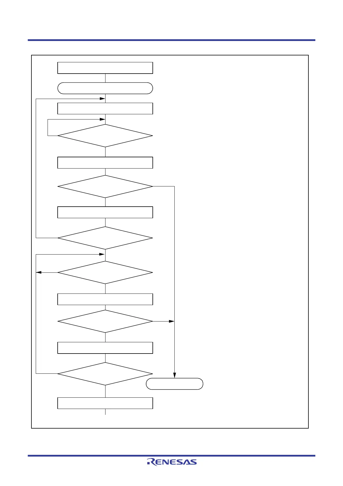
[ 1 ] SCI initialization:
Set data reception.
[ 2 ] ID reception cycle:
Set the MPIE bit in SCR to 1 and wait for ID
reception.
[ 3 ] SCI status confirmation and reception and
comparison of ID:
Read data in RDR at the first RXI interrupt, and
compare it with the ID of the receiving station itself.
If the ID does not match the ID of the receiving
station itself, set the MPIE bit to 1 again, and wait for
another RXI interrupt request.
[ 4 ] Data reception at an RXI interrupt:
Read data in RDR once in the RXI interrupt routine.
[5 ] Receive error processing and break detection:
If a receive error occurs, an error is identified by
reading the ORER and FER flags in SSR. After
performing the appropriate error processing, be sure
to set the ORER and FER flags to 0. Reception
cannot be resumed if any of these flags is set to 1.
In the case of a framing error, a break can be
detected by reading the value of the RXDn pin.
RXI interrupt?
No
ID of receiving station itself?
RXI interrupt?

 Loading...


