R01UH0823EJ0100 Rev.1.00 Page 1054 of 1823
Jul 31, 2019
RX23W Group 33. Serial Communications Interface (SCIg, SCIh)
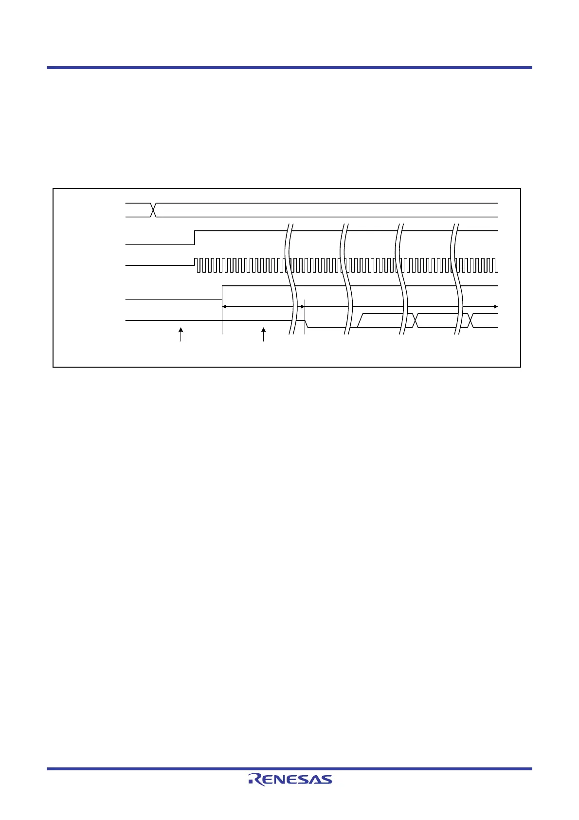
Figure 33.39 shows an example of data transmission when the SCI is set to smart card interface mode according to the
flow described in
Figure 33.38 after a reset. When the pin functions are set to the SCK and TXD pins, they are still
high-impedance because the SCR.CKE[0] and SCR.TE bits are 0. When the CKE[0] bit is set to 1, clock is output from
the SCK pin. When the transmit data is written after setting the TE bit to 1, a data transmission starts. After the TE bit is
set to 1, one frame of high-impedance is output from TXD pin (internal wait time) and then the data transmission starts.
In smart card interface mode, the clock is continuously output while the CKE[0] bit is set to 1 (clock output) even if both
the TE and RE bits are set to 0.
Figure 33.39 Example of Data Transmission Timing in Smart Card Interface Mode
Smart card interface modeMode
SCK pin
Hi-Z
SCR.TE bit
TXD pin
SCR.CKE[0] bit
Hi-Z
D0 D2D1Ds
Wait time Data transmission
Transmit data is writtenPin function is set

 Loading...


