R01UH0823EJ0100 Rev.1.00 Page 1192 of 1823
Jul 31, 2019
RX23W Group 36. CAN Module (RSCAN)
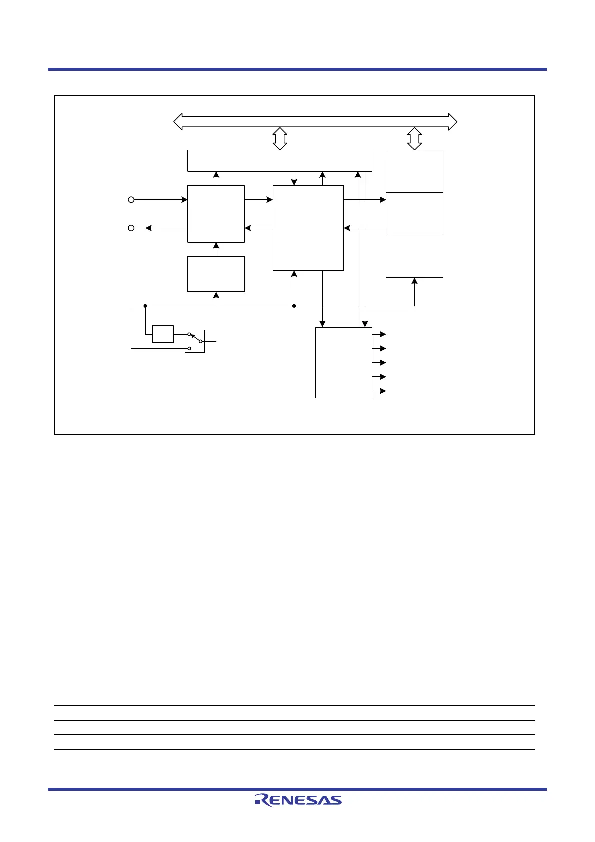
Figure 36.1 CAN Module Block Diagram
CRXD0/CTXD0: CAN input/output pins
Protocol controller: Handles CAN protocol processing such as bus arbitration, bit timing at transmission
and reception, stuffing, and error handling, etc.
Receive rule table RAM: Stores the rules for filtering received messages. Each receive rule specifies an ID/
frame format/data length code of the message to be received, a label to be attached
to the message that has passed through the filter, and the location of such message
to be stored.
FIFO RAM: Includes three 16-stage FIFO buffers. There are two FIFOs for reception only and
one FIFO for transmission or reception.
Buffer RAM: Used as a transmit and receive buffer. There are 4 buffers for transmission and 16
buffers for reception.
Acceptance filter: Performs filtering of received messages.
Timer: There are a timer for timestamp function during reception and a timer which
determines the message transmission intervals while using the transmit FIFO buffer.
Table 36.2 I/O Pins of the CAN Module
Pin Name I/O Description
CRXD0 Input Receive data input pins of the RSCAN0
CTXD0 Output Transmit data output pins of the RSCAN0
CRXD0
CTXD0
fCANTQ
fCAN
Peripheral module
clock (PCLK)
Main clock
(CANMCLK)
Global receive FIFO interrupt
Global error interrupt
Channel transmit interrupt
Transmit/receive FIFO receive interrupt
Channel error interrupt
DCS
Protocol
controller
CAN-related registers
Internal peripheral bus
Receive rule
table RAM
Interrupt
generator
Acceptance filter
ID priority transmit
controller
Timer
Baud rate
prescaler
(BRP[9:0])
BRP[9:0]: Bits in the CFGL register
DCS: Bit in the GCFGL register
fCANTQ: CANTq clock
fCAN: CAN count source
FIFO RAM
Buffer RAM
1/2

 Loading...


