R01UH0823EJ0100 Rev.1.00 Page 1343 of 1823
Jul 31, 2019
RX23W Group 38. Serial Peripheral Interface (RSPIa)
mapped to the single address of SPDR.
Data written to SPDR are written to a transmit-buffer stage (SPTXn) (n = 0 to 3) and then transmitted from the buffer.
The receive buffer holds received data on completion of reception. The receive buffer is not updated if an overrun is
generated.
Furthermore, if the data length is other than 32 bits, bits not referred to in SPTXn (n = 0 to 3) are stored in the
corresponding bits in SPRXn. For example, if the data length is 9 bits, received data are stored in the SPRXn[8:0] bits
and the SPTXn[31:9] bits are stored in the SPRXn[31:9] bits.
(1) Bus Interface
SPDR is the interface with 32-bit wide transmit and receive buffers, each of which has four stages, for a total of 32 bytes.
In other words, the 32 bytes are mapped to the 4-byte address space for SPDR. Furthermore, the unit of access for SPDR
is selected by the SPDCR.SPLW bit.
Data for transmission should be flush with the LSB end of the register. Received data are stored flush with the LSB end.
Operations involved in writing to and reading from SPDR are described below.
(a) Writing
Data written to SPDR are written to a transmit buffer (SPTXn). This is not influenced by the value of the
SPDCR.SPRDTD bit unlike when reading from SPDR.
The transmit buffer includes a transmit buffer write pointer which is automatically updated to indicate the next stage each
time data are written to SPDR.
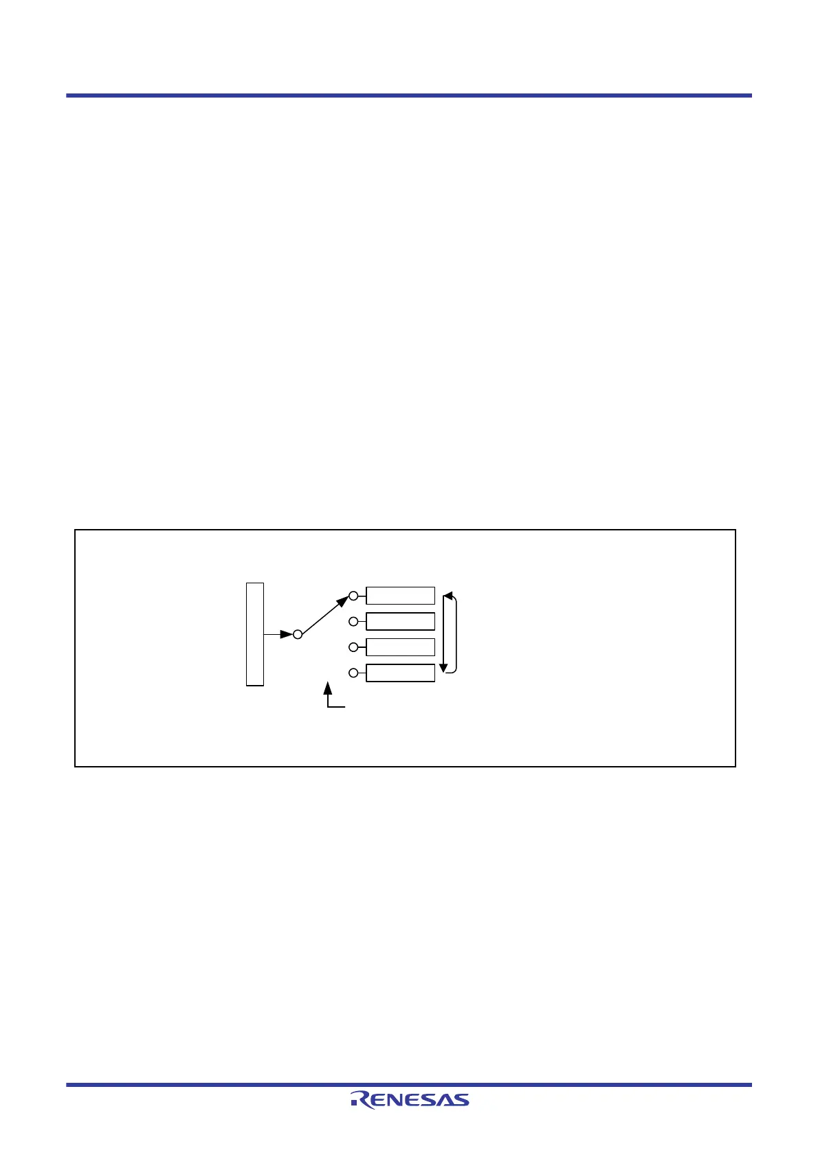
Figure 38.3 shows the configuration of the bus interface with the transmit buffer in the case of writing to SPDR.
Figure 38.3 Configuration of SPDR (Writing)
The sequence for switching the transmit buffer write pointer differs with the setting of the number of frames specification
bits in the RSPI data control register (SPDCR.SPFC[1:0]).
Settings of the SPFC[1:0] bits and sequence of switching the pointer among SPTX0 to SPTX3.
When the SPFC[1:0] bits are 00b: SPTX0 → SPTX0 → SPTX0 → …
When the SPFC[1:0] bits are 01b: SPTX0 → SPTX1 → SPTX0 → SPTX1 → …
When the SPFC[1:0] bits are 10b: SPTX0 → SPTX1 → SPTX2 → SPTX0 → SPTX1 → …
When the SPFC[1:0] bits are 11b: SPTX0 → SPTX1 → SPTX2 → SPTX3 → SPTX0 → SPTX1 → …
When 1 is written to the RSPI function enable bit in the RSPI control register (SPCR.SPE) while the bit’s current value is
0, SPTX0 will be the destination the next time writing proceeds.
When writing to the transmit buffer (SPTXn) after generation of the transmit buffer empty interrupt (after the
SPSR.SPTEF flag becomes 1), write the number of frames set by the number of frames specification bits (SPFC[1:0]) in
SPTX0
SPTX1
SPTX2
SPTX3
SPDR
Write access + Setting of the SPFC[1:0] bits

 Loading...


