R01UH0823EJ0100 Rev.1.00 Page 1344 of 1823
Jul 31, 2019
RX23W Group 38. Serial Peripheral Interface (RSPIa)
the RSPI data control register (SPDCR). Even if the number of frames is written to the transmit buffer (SPTXn), the
value of the buffer is not updated after completion of the writing and before generation of the next transmit buffer empty
interrupt (while the SPSR.SPTEF flag is 0).
(b) Reading
SPDR can be read to read the value of a receive buffer (SPRXn) or a transmit buffer (SPTXn). The setting of the RSPI
receive/transmit data select bit in the RSPI data control register (SPDCR.SPRDTD) selects whether reading is of the
receive or transmit buffer.
The sequence of reading the SPDR register is controlled by independent pointers, receive buffer read pointer and
transmit buffer read pointer.
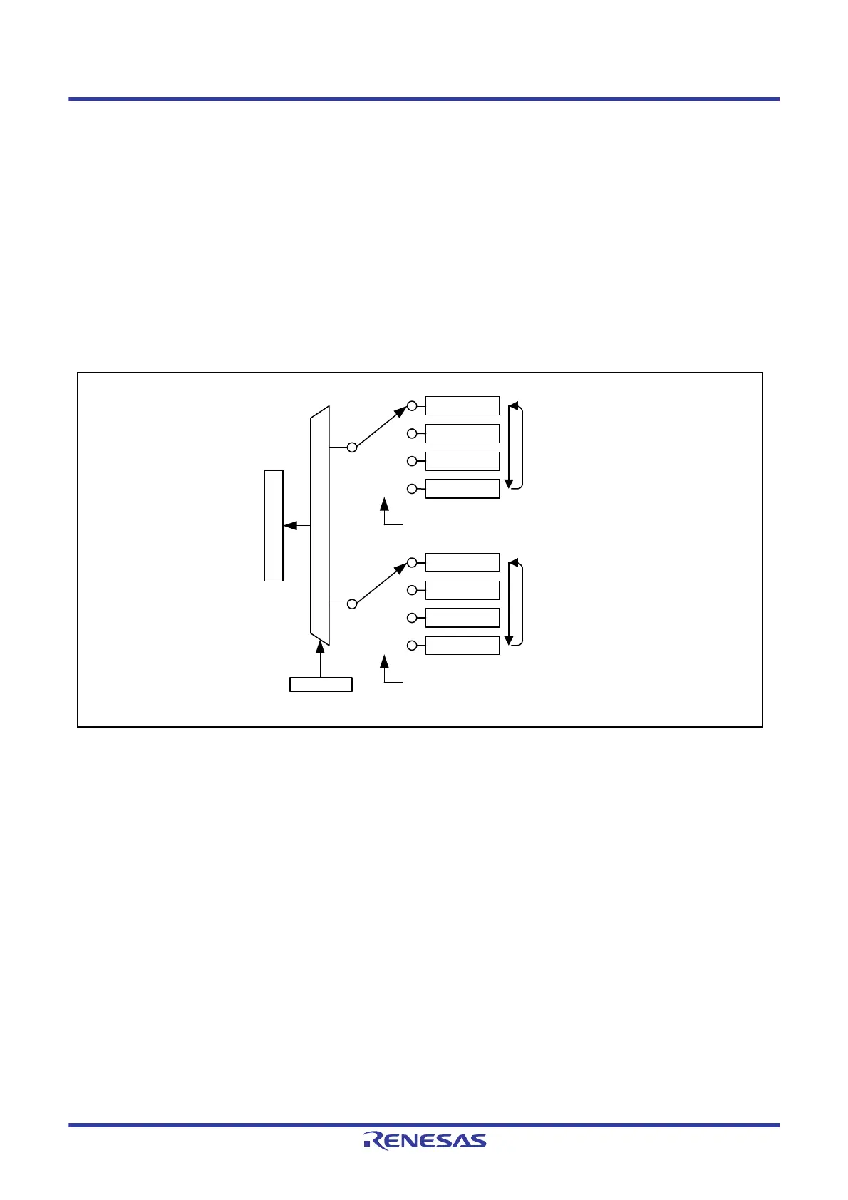
Figure 38.4 shows the configuration of the bus interface with the receive and transmit buffers in the case of reading
from SPDR.
Figure 38.4 Configuration of SPDR (Reading)
Reading the receive buffer switches the receive buffer read pointer to the next buffer automatically.
The sequence of switching the receive buffer read pointer is the same as that for the transmit buffer write pointer.
However, when 1 is written to the RSPI function enable bit in the RSPI control register (SPCR.SPE) while the bit’s
current value is 0, SPRX0 will be indicated by the buffer read pointer the next time reading proceeds.
The transmit buffer read pointer is updated when writing to SPDR, and not updated when reading from the transmit
buffer. When reading from the transmit buffer, the value most recently written to SPDR is read. However, after
generation of the transmit buffer empty interrupt, the values read from the transmit buffer are all 0 in the interval after
completion of writing the number of frames of data specified in the number of frames specification bits
(SPDCR.SPFC[1:0]) and before generation of the next buffer empty interrupt (while the SPSR.SPTEF flag is 0).
SPDR
SPTX0
SPTX1
SPTX2
SPTX3
Read access to transmit buffer +
Setting of the SPFC[1:0] bits
SPRX0
SPRX1
SPRX2
SPRX3
Read access to receive buffer +
Setting of the SPFC[1:0] bits
SPRDTD
0
1

 Loading...


