R01UH0823EJ0100 Rev.1.00 Page 1383 of 1823
Jul 31, 2019
RX23W Group 38. Serial Peripheral Interface (RSPIa)
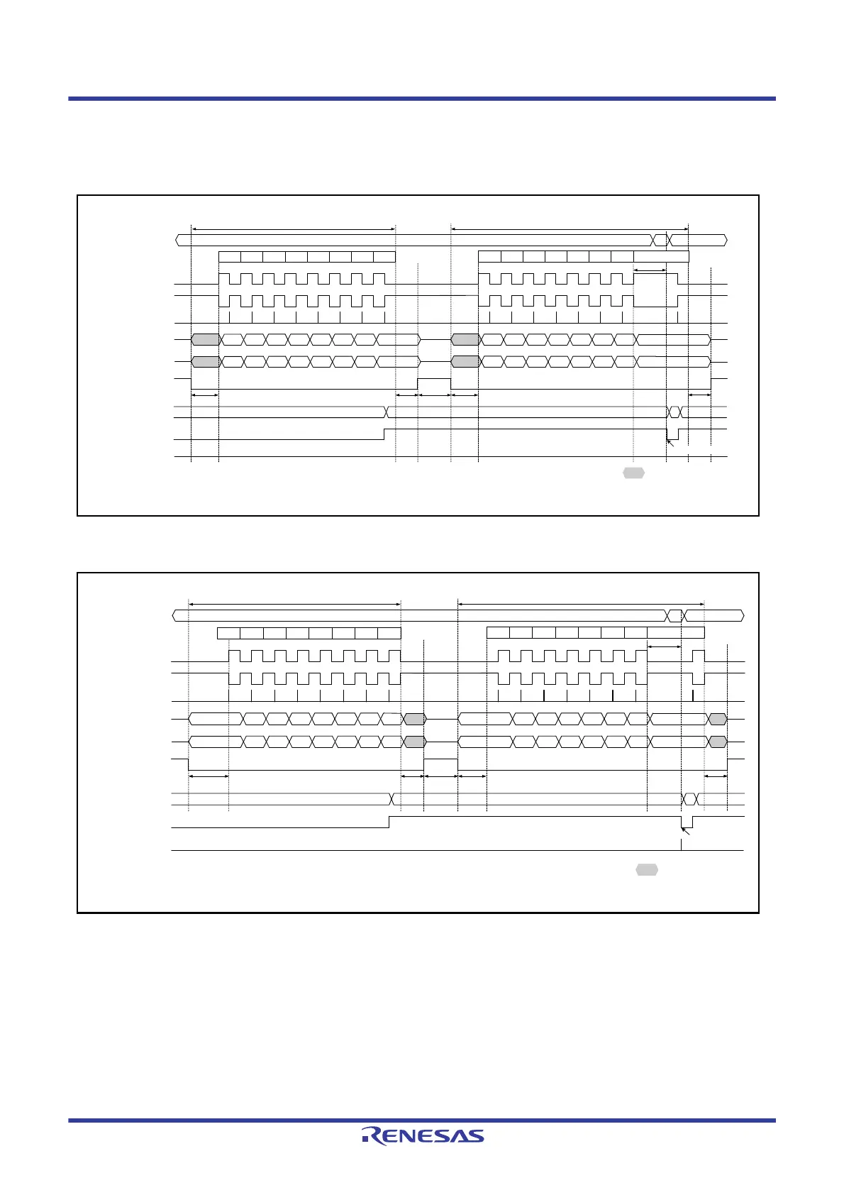
When the RSPCK auto-stop function is enabled in master mode, an overrun error does not occur. Figure 38.28 and
Figure 38.29 show the clock stop waveform when a serial transfer continues while the receive buffer is full in master
mode.
Figure 38.28 Clock Stop Waveform When a Serial Transfer Continues While the Receive Buffer is Full in Master
Mode (CPHA = 1)
Figure 38.29 Clock Stop Waveform When a Serial Transfer Continues While the Receive Buffer is Full in Master
Mode (CPHA = 0)
The operation of the flags at the timings shown in steps (1) and (2) in the figure is described below.
(1) When the receive buffer is full, an overrun error does not occur because the RSPCK clock is stopped.
(2) If SPDR is read while the clock is stopped, data in the receive buffer can be read. The RSPCK clock restarts after
reading the receive buffer (after the SPRF flag becomes 0).
Serial transfer period
RSPCK
cycle
Start
R
t1
t2
Full
1 2 3 4 5 6 7 8
Clock is stopped
Serial transfer period
RSPCK
cycle
Start
End
t1
t2 t3
Empty
1 2 3 4 5 6 7 8
t1: RSPI clock delay register (SPCKD)
t2: RSPI slave select delay register (SSLND)
t3: RSPI next-access delay register (SPND)
RSPI transfer format (CPHA = 1)
output: Undefined (0 or 1)
Input: Don't care
Low
(1)
(2)
End
Em
pty
Full
Receive data is read
RSPCKA
(CPOL = 0)
RSPCKA
(CPOL = 1)
SPDR access
Sampling timing
MOSIA
MISOA
SSLAi
Receive buffer status
SPRF
(Receive buffer full flag)
OVRF
(Overrun error flag)
Serial transfer period
RSPCK
cycle
Start
End
t1
t2
Full
1 2 3 4 5 6 7 8
Clock is stopped
Serial transfer period
RSPCK
cycle
Start
End
t1
t2 t3
Empty
1 2 3 4 5 6 7 8
RSPI transfer format (CPHA = 1)
output: Undefined (0 or 1)
Input: Don't care
Low (1)
R
(2)
t1: RSPI clock delay register (SPCKD)
t2: RSPI slave select delay register (SSLND)
t3: RSPI next-access delay register (SPND)
Empt
y
Full
Receive data is read
RSPCKA
(CPOL = 0)
RSPCKA
(CPOL = 1)
SPDR access
Sampling timing
MOSIA
MISOA
SSLAi
OVRF
(Overrun error flag)
SPRF
(Receive buffer full flag)
Receive buffer
status

 Loading...


