R01UH0823EJ0100 Rev.1.00 Page 1601 of 1823
Jul 31, 2019
RX23W Group 44. 12-Bit A/D Converter (S12ADE)
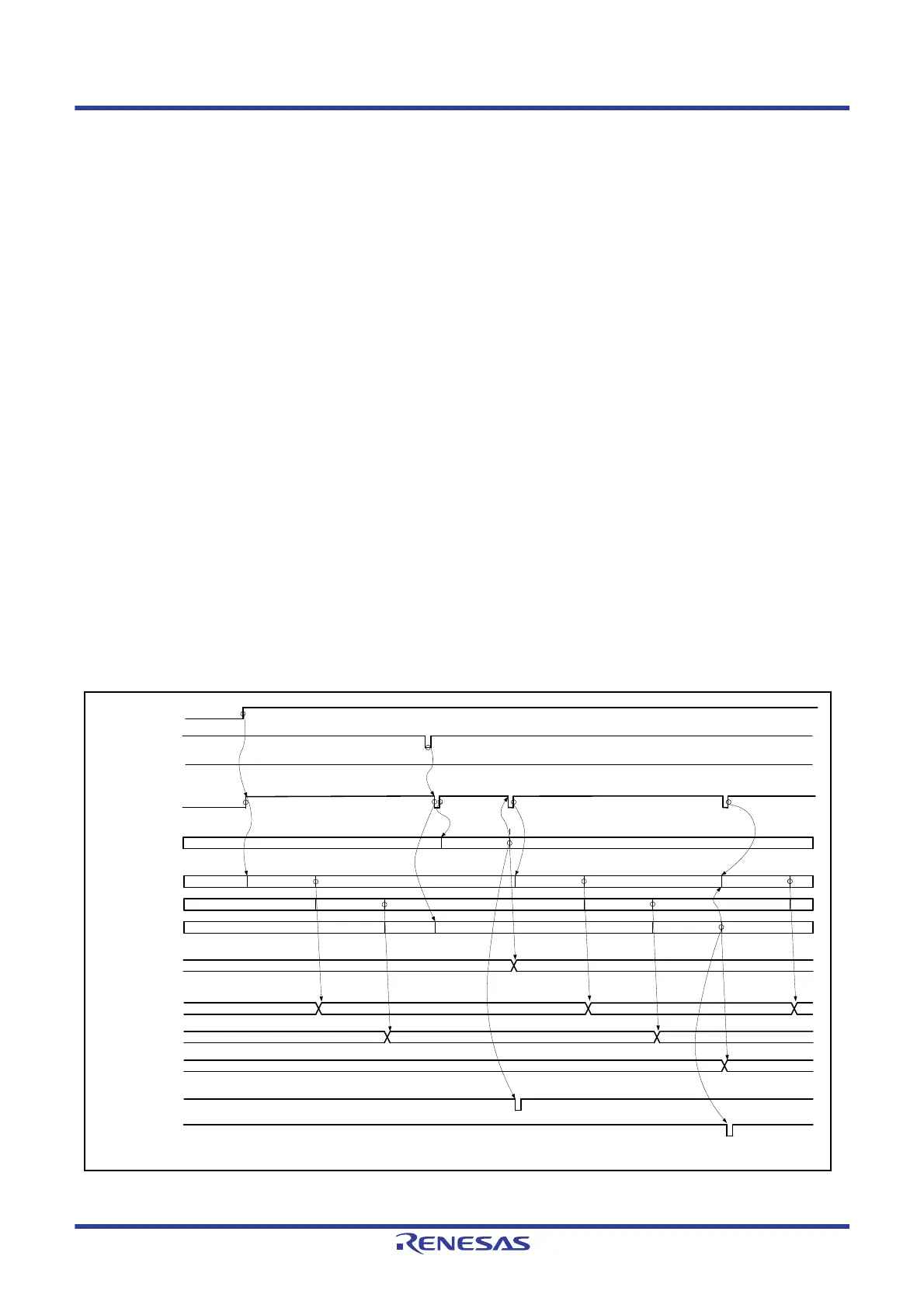
The following is an example of operation under group-A priority control in which channel 0 is selected for group A and
channels 1 to 3 are selected for group B (ADGSPCR.GBRP = 1).
(1) The ADCSR.ADST bit is set to 1 (A/D conversion start) when ADGSPCR.GBRP is set to 1, and conversion for the
ANn channels selected in the ADANSB0 and ADANSB1 registers, starting from the channel with the smallest
number n.
(2) On completion of A/D conversion on a single channel, the result is stored in the corresponding A/D data register (ADDRy).
(3) If a group A trigger is input during A/D conversion on group B, the ADCSR.ADST bit is cleared to 0 and the
ongoing A/D conversion on group B is stopped. After that, the ADCSR.ADST bit is set to 1 (A/D conversion start)
and conversion for the ANn channels selected in the ADANSA0 and ADANSA1 registers, starting from the channel
with the smallest number n.
(4) On completion of A/D conversion on a single channel, the result is stored in the corresponding A/D data register (ADDRy).
(5) An S12ADI0 interrupt request is generated if the setting of the ADCSR.ADIE bit is 1 (S12ADI0 interrupt upon
scanning completion enabled).
(6) After the ADST bit is automatically cleared, again, the ADCSR.ADST bit is automatically set to 1 (A/D conversion
start) and conversion for the ANn channels selected in the ADANSB0 and ADANSB1 registers, starting from the
channel with the smallest number n.
(7) On completion of A/D conversion on a single channel, the result is stored in the corresponding A/D data register (ADDRy).
(8) A GBADI interrupt request is generated if the setting of the ADCSR. GBADIE bit is 1.
(9) After the ADST bit is automatically cleared, again, the bit is automatically set to 1 (A/D conversion start) and
conversion for the ANn channels selected in the ADANSB0 and ADANSB1 registers, starting from the channel
with the smallest number n. Steps 6 to 9 are repeated as long as the ADGSPCR.GBRP bit remains 1.
Clearing of the ADCSR.ADST bit to 0 is prohibited while the ADGSPCR.GBRP bit is set to 1. To forcibly stop
A/D conversion when ADGSPCR.GBRP = 1, follow the procedures for clear operation by software through the
ADCSR.ADST bit shown in
section 44.8.2, Notes on Stopping A/D Conversion.
Figure 44.18 Example of Operation under Group-A Priority Control (5) (when ADGSPCR.GBRP = 1)
Channel 1 (AN001) Waiting for conversion
Channel 2 (AN002) Waiting for conversion
Channel 3 (AN003) Waiting for conversion
ADDR1
ADDR2
ADDR3
A/D conversion B1
Stored
A/D conversion B2
Waiting for conversion
Waiting for conversion
A/D conversion B3*
1
A/D conversion result B1
A/D conversion result B2
A/D conversion result B4
Interrupt generated
Waiting for conversion
ADST
A/D
conversion
started
Waiting for conversion
ADDR0
Result of A/D conversion A1
Interrupt generated
A/D conversion A1
Channel 0 (AN000)
A/D conversion B4
A/D conversion B5
Waiting for conversion
A/D conversion B6
Waiting for conversion
Waiting for conversion
A/D conversion result B5
Trigger for group B
Trigger for group A
Group A
Group B
Waiting for conversion
GBADI
(8)
A/D conversion B7
Stored
GBRP
(1)
(2)
Stored (2)
Stored (4)
Stored (7)
(3)
(6)
Stored (7)
Stored (7)
A/D conversion result B6
(5)
(9)
Note 1. The converted data of A/D conversion B3 are ignored.

 Loading...


