R01UH0823EJ0100 Rev.1.00 Page 1702 of 1823
Jul 31, 2019
RX23W Group 50. Flash Memory (FLASH)
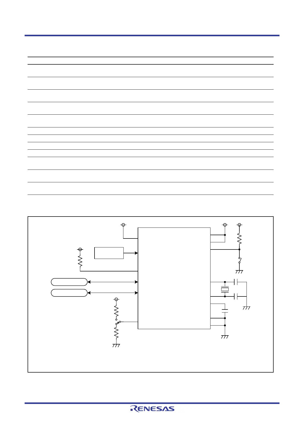
Figure 50.23 Example of Pin Connections in Boot Mode (USB Interface) When Bus-Powered
Table 50.8 Pin Handling in Boot Mode (USB Interface) When Self-Powered
Pin Name Name I/O Function
VCC, VSS Power supply — Input the voltage between 3.0 V and 3.6 V to the VCC pin.
Input 0 V to the VSS pin.
VCC_USB, VSS_USB USB power supply — Connect the VCC_USB pin to the VCC pin.
Connect the VSS_USB pin to the VSS pin.
AVCC0, AVSS0 12-bit A/D converter power
supply
— Connect the AVCC0 pin to the VCC pin.
Connect the AVSS0 pin to the VSS pin.
VCL Decoupling capacitor connect
pin
— Connect to the VSS pin via a decoupling capacitor for stabilizing
the internal voltage.
XTAL, EXTAL Main clock I/O pin I/O Connect a 4, 6, 8, 12, or 16 MHz crystal or ceramic resonator or
oscillator.
MD Operating mode control Input Input low.
PC7/UB Operating mode control Input Input high.*
1
P35/UPSEL USB power mode control Input Input low.
RES# Reset input Input Reset pin. Connect to the reset circuit.
USB0_DP USB on-chip transceiver D+
I/O pin
I/O Connect to the circuit described in section 32, USB 2.0
Host/Function Module (USBc).
USB0_DM USB on-chip transceiver D–
I/O pin
I/O Connect to the circuit described in section 32, USB 2.0
Host/Function Module (USBc).
P16/USB0_VBUS USB cable connection
monitor pin
Input Connect to the circuit described in section 32, USB 2.0
Host/Function Module (USBc).
Note 1. Maintain the input level for 2 ms or longer after a reset is released.
MCU
VCC
USB0_VBUS
VCC_USB
UPSEL
RES#
UB
USB0_DP XTAL
USB0_DM
EXTAL
VCL
VSS_USB
MD
VSS
Reset circuit
(User logic)
Data I/O
Data I/O
*1
*2
Note 1. Connect a 4, 6, 8, 12, or 16 MHz crystal, ceramic resonator or oscillator to the main clock oscillator.
Note 2. UPSEL is assigned to the same pin as NMI. This is an example when the falling edge is selected by the NMI
detection set bit.

 Loading...


