R01UH0823EJ0100 Rev.1.00 Page 1760 of 1823
Jul 31, 2019
RX23W Group 51. Electrical Characteristics
Note 1. This excludes the CLKOUT_RF pin.
Note 1. This excludes the CLKOUT_RF pin.
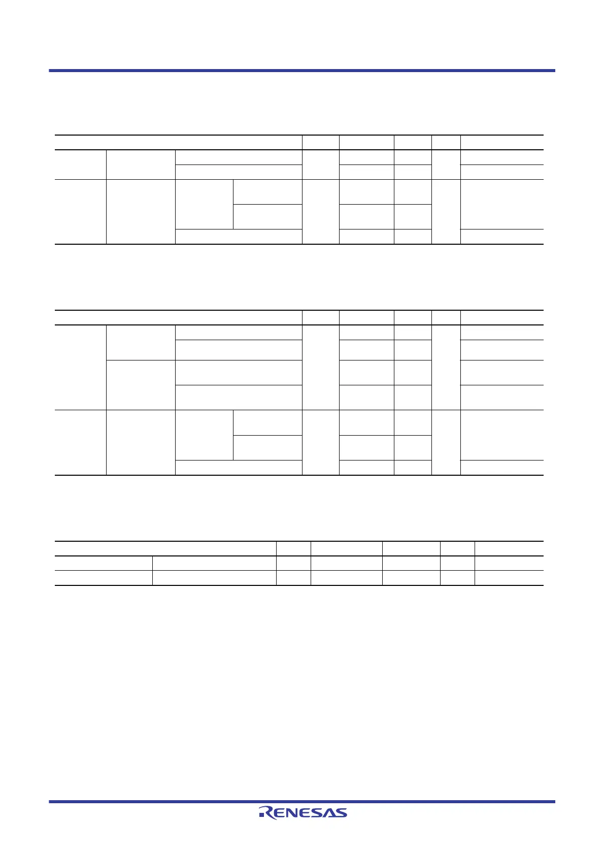
Table 51.18 Output Values of Voltage (1)
Conditions: 1.8 V ≤ VCC = VCC_USB = AVCC0 = VCC_RF = AVCC_RF ≤ 2.7 V, VSS = AVSS0 = VSS_USB = VSS_RF = 0 V,
T
a
= –40 to +85°C
Item Symbol Min. Max. Unit Test Conditions
Output low All output ports*
1
Normal output mode V
OL
—0.8VI
OL
= 0.5 mA
High-drive output mode — 0.8 I
OL
= 1.0 mA
Output high All output ports*
1
Normal output
mode
Ports 03, 05, 07,
Ports 40 to 47
V
OH
AVCC0 – 0.5 — V I
OH
= –0.5 mA
Ports other than
above
VCC – 0.5 —
High-drive output mode VCC – 0.5 — I
OH
= –1.0 mA
Table 51.19 Output Values of Voltage (2)
Conditions: 2.7 V ≤ VCC = VCC_USB = AVCC0 = VCC_RF = AVCC_RF ≤ 3.6 V, VSS = AVSS0 = VSS_USB = VSS_RF = 0 V,
T
a
= –40 to +85°C
Item Symbol Min. Max. Unit Test Conditions
Output low All output ports
(except for RIIC)
*
1
Normal output mode V
OL
—0.8VI
OL
= 1.0 mA
High-drive output mode — 0.8 I
OL
= 2.0 mA
RIIC pins Standard mode (Normal output
mode)
—0.4 I
OL
= 3.0 mA
Fast mode (High-drive output
mode)
—0.6 I
OL
= 6.0 mA
Output high All output ports*
1
Normal output
mode
Ports 03, 05, 07,
Ports 40 to 47
V
OH
AVCC0 – 0.8 — V I
OH
= –1.0 mA
Ports other than
above
VCC – 0.8 —
High-drive output mode VCC – 0.8 — I
OH
= –2.0 mA
Table 51.20 Output Values of Voltage (3)
Conditions: 3.0V ≤ VCC = VCC_USB = AVCC0 = VCC_RF = AVCC_RF ≤ 3.6V, VSS = AVSS0 = VSS_USB = VSS_RF = 0V,
Ta = –40 to +85°C
Item Symbol Min. Max. Unit Test Conditions
Output low CLKOUT_RF V
OL
—0.3VI
OL
= 0.5 mA
Output high CLKOUT_RF V
OH
VCC_RF – 0.3 — V I
OH
= –0.5 mA

 Loading...


