R01UH0823EJ0100 Rev.1.00 Page 530 of 1823
Jul 31, 2019
RX23W Group 23. Multi-Function Timer Pulse Unit 2 (MTU2a)
(3) Selecting Timing for Transfer from Buffer Registers to Timer General Registers in Buffer
Operation
The timing for transfer from buffer registers to timer general registers can be selected in PWM mode 1 or 2 for MTU0 or
in PWM mode 1 for MTU3 and MTU4 by setting the timer buffer operation transfer mode registers (MTU0.TBTM,
MTU3.TBTM, and MTU4.TBTM). Either compare match (initial setting) or TCNT clearing can be selected for the
transfer timing. TCNT clearing as transfer timing is one of the following cases.
When the TCNT counter overflows (FFFFh → 0000h)
When 0000h is written to the TCNT counter during counting
When the TCNT counter is set to 0000h under the condition specified in the TCR.CCLR[2:0] bits
Note: The TBTM register must be modified only while the TCNT counter stops.
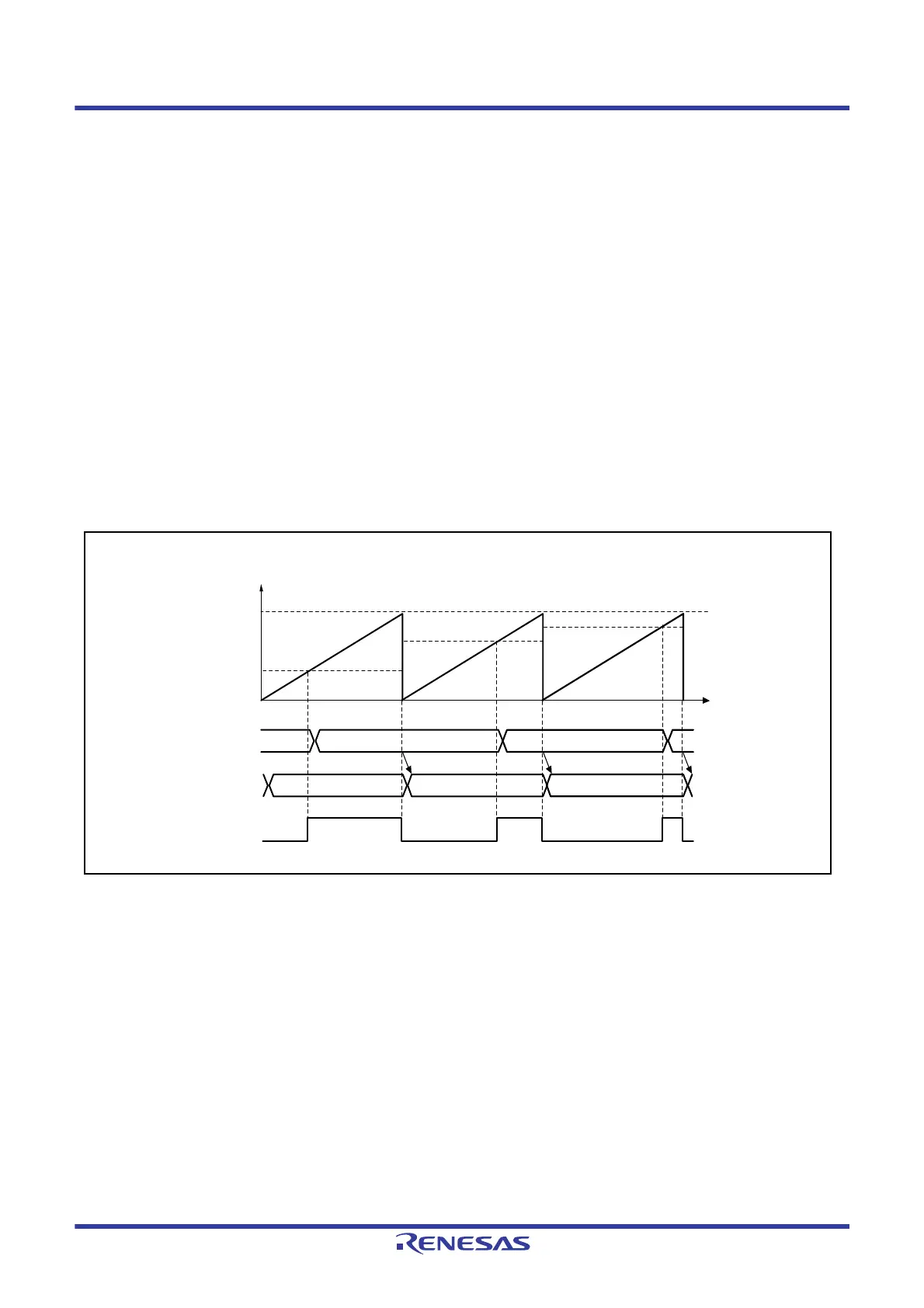
Figure 23.19 shows an operation example in which PWM mode 1 is designated for MTU0 and buffer operation is
designated for registers MTU0.TGRA and MTU0.TGRC. The settings used in this example are MTU0.TCNT clearing
by compare match B, high output at compare match A, and low output at compare match B. The MTU0.TBTM.TTSA bit
is set to 1.
Figure 23.19 Example of Buffer Operation When MTU0.TCNT Clearing is Selected for
MTU0.TGRC-to-MTU0.TGRA Transfer Timing
Time
0520h
0520h
0450h
0450h
0200h
0520h0450h0200h
0200h
Transfer
MTU0.TCNT value
0000h
MTIOC0A
MTU0.TGRA
MTU0.TGRC
MTU0.TGRB
MTU0.TGRA

 Loading...


