R01UH0823EJ0100 Rev.1.00 Page 565 of 1823
Jul 31, 2019
RX23W Group 23. Multi-Function Timer Pulse Unit 2 (MTU2a)
Figure 23.53 Example of 0% and 100% Waveform Output in Complementary PWM Mode (5)
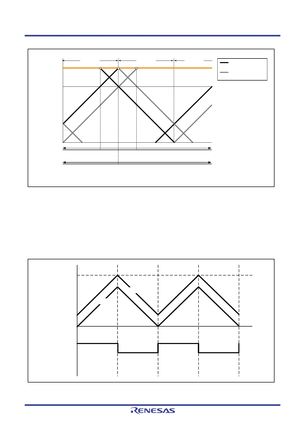
(l) Toggle Output Synchronized with PWM Cycle
In complementary PWM mode, toggle output from the PWM output pin in synchronization with the PWM period can be
enabled by setting the TOCR1.PSYE bit to 1. An example of a toggle output waveform is shown in
Figure 23.54.
This output is toggled by a compare match between the MTU3.TCNT counter and the MTU3.TGRA register and a
compare match between the MTU4.TCNT counter and 0000h.
The MTIOC3A pin is assigned for this toggle output. The initial output is a high level.
Figure 23.54 Example of Toggle Output Waveform Synchronized with PWM Output
MTU3.TCNT
cadb
MTU3.TGRA
TCDRA
TDDRA
0000h
Positive-phase
output
Negative-phase
output
MTU4.TCNT
Output waveform is active-low.
Buffer operation is set for transfer at the crest and trough.
MTU4.TGRA
100% duty cycle output
0% duty cycle output
OFF
Don't care
Don't care
T1 interval T2 interval T1 interval
Counter for generating
a turn-off timing
Counter for generating
a turn-on timing
MTU3.TGRA
0000h
Toggle output
MTIOC3A pin
MTU4.TCNT
MTU3.TCNT

 Loading...


