R01UH0823EJ0100 Rev.1.00 Page 1474 of 1823
Jul 31, 2019
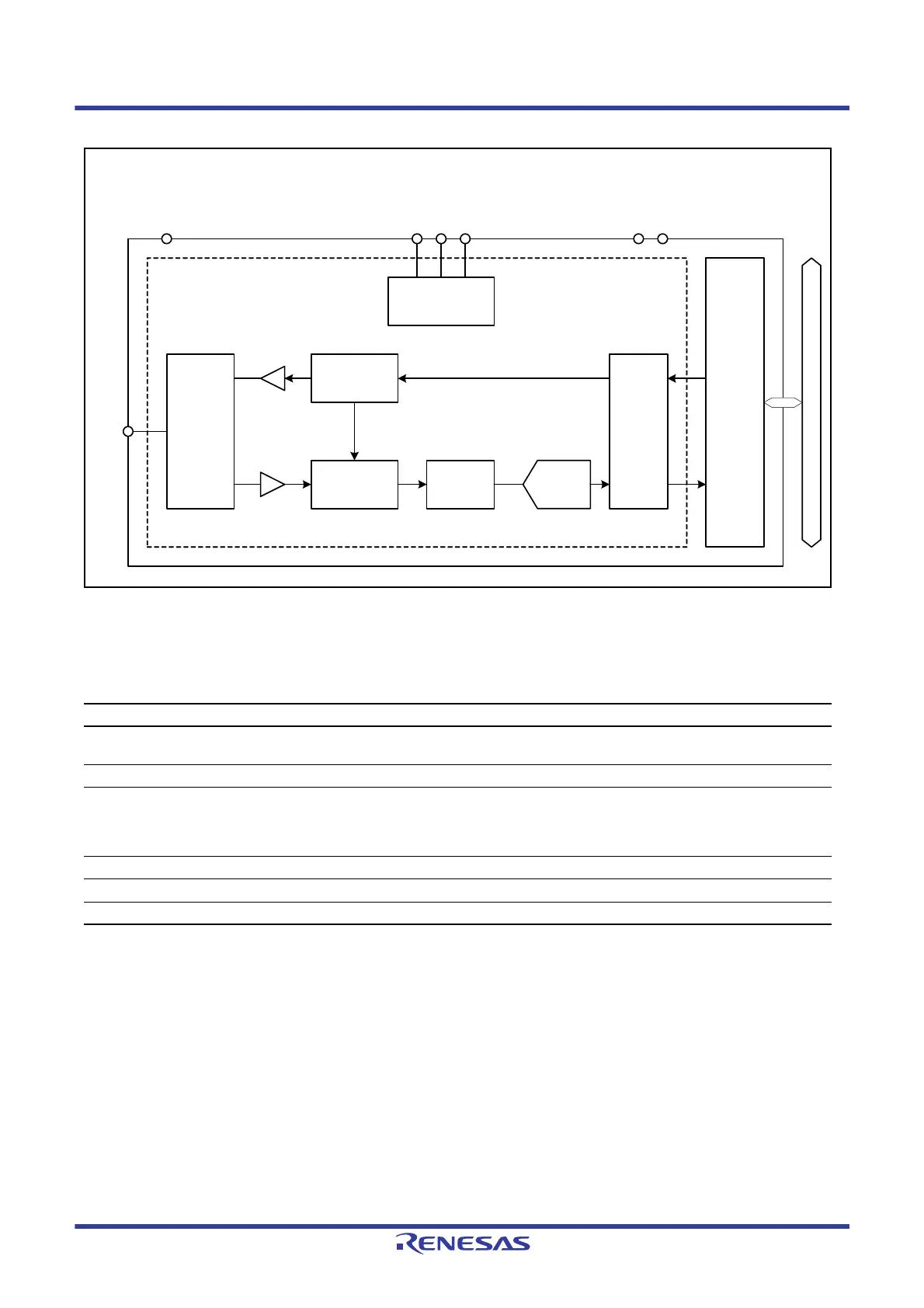
RX23W Group 41. Bluetooth Low Energy (BLE)
Figure 41.1 BLE Block Diagram
Table 41.2 lists the BLE I/O Pins.
Table 41.2 BLE I/O Pins
Pin name I/O Description
ANT I/O RF single I/O pin for RF transceiver
Set the impedance of the signal line to 50 Ω.
DCLOUT Output Output pin for the RF transceiver power-supply
DCLIN_A,
DCLIN_D
Input If the DC-to-DC converter is to be selected as the power supply for the RF transceiver, connect
an inductor and capacitor between the DCLOUT pin and the converter.
If the linear regulator is to be selected as the power supply for the RF transceiver, connect a
capacitor between the DCLOUT pin and the converter.
VCC_RF Input RF transceiver power-supply pin
AVCC_RF Input RF transceiver power-supply pin
VSS_RF Input RF transceiver ground pin
RF transceiver
power-supply
PLL
Frequency
mixer
Low-pass
filter
A/D
converter
Modem
Link
layer
Matching
circuit
RF Transceiver Block
Low noise
amplifier
Power
amplifier
ANT
AVCC_RF
DCLOUT
DCLIN_A
DCLIN_D
VCC_RF
VSS_RF
Internal peripheral bus

 Loading...


