R01UH0823EJ0100 Rev.1.00 Page 1758 of 1823
Jul 31, 2019
RX23W Group 51. Electrical Characteristics
Note 1. When OFS1.(FASTSTUP, LVDAS) bits are 11b.
Note 2. When OFS1.(FASTSTUP, LVDAS) bits are 01b.
Note 3. When OFS1.LVDAS bit is 0.
Note 4. Turn on the power supply voltage according to the normal startup rising gradient because the settings in the OFS1 register are
not read in boot mode.
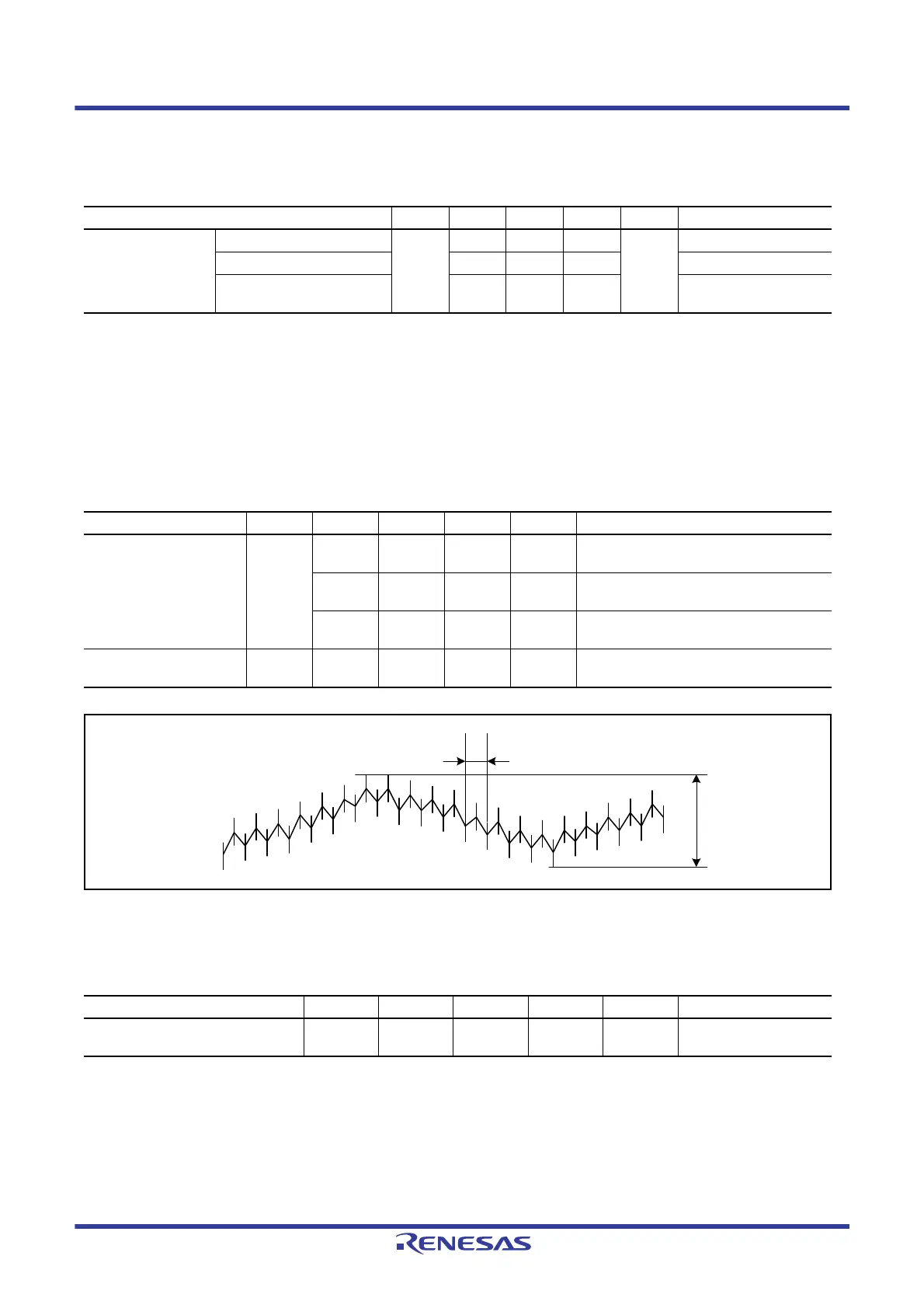
Figure 51.7 Ripple Waveform
Note: The recommended capacitance is 4.7 μF. Variations in connected capacitors should be within the above range.
Table 51.14 DC Characteristics (12)
Conditions: 0 V ≤ VCC = VCC_USB = AVCC0 = VCC_RF = AVCC_RF ≤ 3.6 V, VSS = AVSS0 = VSS_USB = VSS_RF = 0 V,
T
a
= –40 to +85°C
Item Symbol Min. Typ. Max. Unit Test Conditions
Power-on VCC rising
gradient
At normal startup*
1
SrVCC 0.02 — 20 ms/V
During fast startup time*
2
0.02 — 2
Voltage monitoring 0 reset
enabled at startup*
3,
*
4
0.02 — —
Table 51.15 DC Characteristics (13)
Conditions: 1.8 V ≤ VCC = VCC_USB = AVCC0 = VCC_RF = AVCC_RF ≤ 3.6 V, VSS = AVSS0 = VSS_USB = VSS_RF = 0 V,
T
a
= –40 to +85°C
The ripple voltage must meet the allowable ripple frequency f
r (VCC)
within the range between the VCC upper limit and lower limit.
When VCC change exceeds VCC ±10%, the allowable voltage change rising/falling gradient dt/dVCC must be met.
Item Symbol Min. Typ. Max. Unit Test Conditions
Allowable ripple frequency f
r (VCC)
— — 10 kHz Figure 51.7
V
r (VCC)
≤ VCC × 0.2
— — 1 MHz Figure 51.7
V
r (VCC)
≤ VCC × 0.08
— — 10 MHz Figure 51.7
V
r (VCC)
≤ VCC × 0.06
Allowable voltage change
rising/falling gradient
dt/dVCC 1.0 — — ms/V When VCC change exceeds VCC ±10%
Table 51.16 DC Characteristics (14)
Conditions: 1.8 V ≤ VCC = VCC_USB = AVCC0 = VCC_RF = AVCC_RF ≤ 3.6 V, VSS = AVSS0 = VSS_USB = VSS_RF = 0 V,
T
a
= –40 to +85°C
Item Symbol Min. Typ. Max. Unit Test Conditions
Permissible error of VCL pin external
capacitance
C
VCL
1.4 4.7 7.0 μF

 Loading...


