R01UH0823EJ0100 Rev.1.00 Page 534 of 1823
Jul 31, 2019
RX23W Group 23. Multi-Function Timer Pulse Unit 2 (MTU2a)
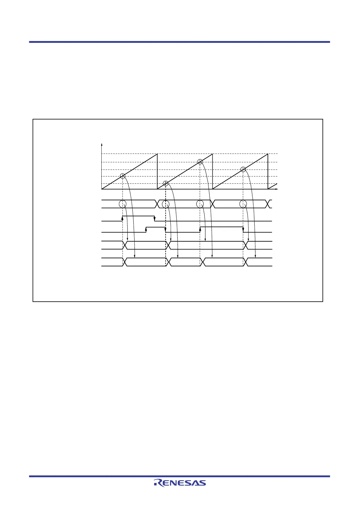
(4) Cascaded Operation Example (c)
Figure 23.23 illustrates the operation when counters MTU1.TCNT and MTU2.TCNT have been cascaded and the I2AE
and I1AE bits in TICCR register have been set to 1 to include the MTIOC2A and MTIOC1A pins in the MTU1.TGRA
and MTU2.TGRA input capture conditions, respectively. In this example, the IOA[3:0] bits in both MTU1.TIOR and
MTU2.TIOR registers have selected both the rising and falling edges for the input capture timing. Under these
conditions, the OR result of MTIOC1A and MTIOC2A input is used for the MTU1.TGRA and MTU2.TGRA input
capture conditions.
Figure 23.23 Cascaded Operation Example (c)
MTU2.TCNT value
Time
0514h
0514h
0513h0512h
0513h0512h
C256h
6128h 2064h 9192h
0000h
MTU1.TGRA
MTU2.TGRA
MTIOC1A
MTIOC2A
MTU1.TCNT
C256h
FFFFh
6128h
2064h
9192h
Note 1. When either input signal is at the high level, an edge in the other input signal does not act as the
condition for capture.
*
1
*
1

 Loading...


